

Gordon Moore was Research Director at Fairchild Semiconductors in 1965 when he was asked to predict the next 10 years’ development in the semiconductor industry. Moore noticed the number of components on a chip seemed to double every year. Moore’s Law was born.

10 years later, during which Moore co-founded Intel, he revisited his prediction. The fast pace with which the number of components had doubled was slowing down a bit, so Moore predicted the doubling of components would happen every second year.


Since then, Moore’s Law has been a good approximation for the development of chips. “More Moore” has been the mantra when members of the Semiconductor Industry Association (SIA) such as Intel, AMD, Samsung and IBM planned the next generation of chips.

The Death of a Law
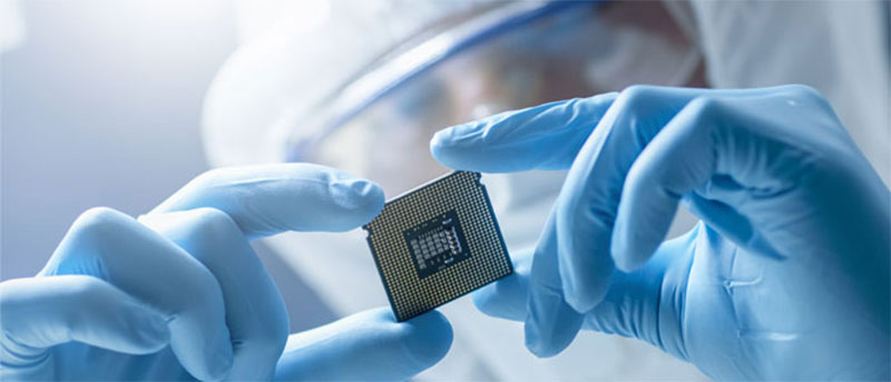
But then something happened. The now microscopic components, measured in nanometers, are causing problems. Intel’s current Broadwell-architecture is based on 14 nanometre-technology and the upcoming Cannonlake is based on 10 nanometre-technology. The light used in the manufacturing process has a wavelength of 193 nanometers.
Yes, that makes things difficult. Not quite impossible, but a very difficult manufacturing process is required which is prone to delays. Broadwell was delayed and Cannonlake is as well.
Last year, SIA announced that the “More Moore” will be replaced with a “More than Moore” approach to chip manufacturing. Instead of focusing purely on doubling the number of chip-components, other factors, such as power consumption, are important as well.
This doesn’t mean that the chip development has stalled. In particular, AI is driving interesting chip design.
Microsoft uses FPGA in Azure
Microsoft has started to roll out FPGA-chips (Field Programmable Gate Arrays) on Azure. FPGAs are not traditional general purpose CPUs. As the name implies, you can program FPGAs, but it is done by programming and reconfiguring logic blocks, that can be simple boolean operations such as AND and XOR or more complex logical operations.
This is done in hardware description languages such VHDL and Verilog, although there are efforts to make FPGA-programming more accessible for high-level languages. FPGAs are faster than CPUs and use less power which makes them interesting in the compute-intensive AI-field.
You can watch Microsoft’s Mark Russinovich, CTO for Azure, talk about the plans for FPGAs on Azure at https://channel9.msdn.com/Events/Build/2017/B8063. Microsoft has used FPGA from the manufacturer Altera for quite a while. They were first used to speed up Bing’s search algorithms. Microsoft’s interest in FPGA-chips made Intel very interested in FPGA too. The interest ended with Intel buying Altera in December 2015 for 16.7 billion dollars.
Google manufactures own chip
Another player in cloud computing, Google, decided to develop its own chips, TPUs (Tensor Processing Units). The TPUs are actually ASICs (Application Specific Integrated Circuit), which means they are manufactured specifically for one purpose. As the name implies, they are designed for Google’s Tensorflow, which is an open source framework for machine learning.
In May 2017, Google revealed the second generation of TPUs. Each TPU is equipped with network-capabilities which makes it possible to combine TPUs in something Google calls a TPU pod.
Each TPU pod consists of 64 second-generation TPUs, which gives a combined computing power up to 11.5 petaflops.
Amazon and NVIDIA-chips
Just as Google and Microsoft have started to look at alternatives to CPUs in order to provide speed for Machine Learning, so has the biggest cloud platform, Amazon’s AWS. They have teamed up with NVIDIA to use GPU’s (Graphics Processing Unit) which were originally cherished by gamers because of the GPUs ability to render fast-moving graphics. The GPUs’ inherent parallel processing of data has in recent years made them very popular for AI-research and AI-systems.
May 2017, Amazon announced a renewed collaboration with NVIDIA, AWS-users will get access to NVIDIAs new GPU-architecture Volta, which will replace the current Pascal-chip.
According to NVIDIA, Volta will be able to give up to 100 teraflops, which will increase the deep learning performance with a factor 5.
IBM’s brain-inspired Chip
Yet another player in the AI-field is IBM, whose Watson primarily is based on traditional CPUs in the form of IBM’s own Power-chips. Recently, IBM announced a cooperation with Nvidia to offer Nvidia Pascal GPUs in IBM’s Bluemix cloud.
But IBM is also getting a totally different chip-technology ready for AI.
In the successful AI-implementations of today, it is the practical results that count. Whether the convolutional neural networks used in Machine Learning are working precisely, or even just slightly, as the human brain really doesn’t matter.
The important thing is that the neural networks facial recognition is as good as or better than humans.
In computational neuroscience, there’s a different approach where models inspired by the human brain are the design principle. This approach has inspired IBM’s TrueNorth-chip. The TrueNorth-chip has one million programmable neurons and 256 million programmable synapses connecting the neurons. Maybe that sounds impressive, but the human brain has around 100 billion neurons and between 100 trillion (1012) and 1 quadrillion synapses (1015), so we are far from even a simple model of the brain.
Anyway, TrueNorth operates with 4096 neurosynaptic cores, each of them equipped with memory, computational unit and communication. Until recently, TrueNorth has not been able to use the well-established convolutional neural networks, but last year IBM announced that TrueNorth is capable of using them.
Maybe Moore’s Law is dead, but the chip revolution is continuing!