

A key milestone for advanced chip design, highlighting India’s growing role in next-generation semiconductor innovation under Semicon Mission 2.0.


Qualcomm’s successful design and tape-out of a 2-nanometre semiconductor chip — with significant contribution from its Indian engineering centres — marks a landmark moment for India’s semiconductor ecosystem, underscoring a shift from services to high-end product development. The advanced 2nm chip, unveiled in Bengaluru in the presence of Union Minister Shri Ashwini Vaishnaw, houses tens of billions of transistors and integrates both a CPU and GPU, potentially powering AI-enabled devices from cameras to autonomous vehicles.
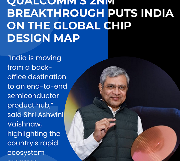
Vaishnaw said the development reflects India’s progress toward an end-to-end semiconductor capability, moving beyond back-office roles to full chip design, tape-out and validation, aligning with the government’s broader vision under the Semicon India Mission. The breakthrough comes as India prepares to launch Semicon India Mission 2.0, which will prioritise semiconductor design, equipment and materials manufacturing, talent development, and advanced fabrication technologies such as 7nm nodes.
The achievement also highlights India’s growing talent pipeline and design ecosystem, with thousands of engineers trained and hundreds of universities offering cutting-edge semiconductor programmes. Industry analysts say this 2nm milestone could catalyse deeper investment and partnerships, helping India strengthen its position in the global semiconductor value chain.