

Publishing their findings in Nanotechnology in a paper titled “Three fundamental devices in one: a reconfigurable multifunctional device in two-dimensional WSe 2“, the researchers detail how they were able to develop new doping strategies with this recently discovered transition metal dichalcogenide semiconductor to yield novel behaviours.
Aiming to reduce fabrication complexity and footprint, the researchers designed a reconfigurable device that can morph into three fundamental semiconductor devices: a p-n diode (rectifier), a MOSFET (for switching), and a bipolar junction transistor (for current amplification).


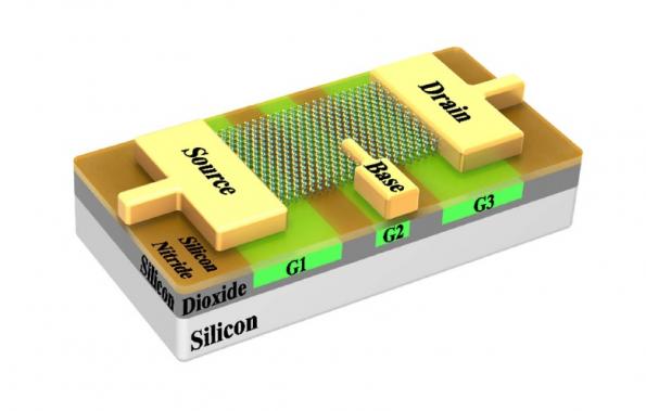
While such devices would typically be fabricated individually on modern chips, each requiring complex integration step, here the multiple functions device relies on multiple buried gates to achieve n- and p-channels, in effect dynamically selecting which carriers (electrons or holes) flow at the surface of the semiconductor.

This novel reconfigurable doping technique means a single device can be architected so as to operate differently depending on how the gates are controlled. After building their first proof-of-concept device, the researchers hope to implement such multifunctional devices into electronic circuits that would be more compact and simpler to manufacture than CMOS-based devices.