

- Builds on agentic AI capabilities introduced at DAC 2026, extending them to 3D integrated circuits (3D IC) electrothermal codesign
- Orchestrates nine automated workflow stages across seven of Siemens’ electronic design automation (EDA) tools, reducing setup effort by up to 95 percent
- Enables evaluation of up to 50x as many design alternatives to address power and thermal constraints in advanced 3D IC packages for AI computing
- Part of an expanding portfolio of long-running, self-verifying agentic AI workflows across the EDA design flow
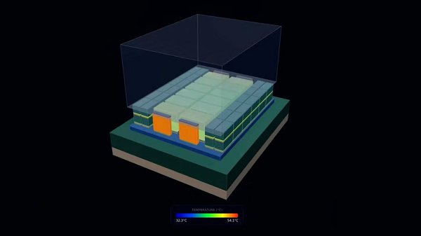

Siemens today announced an expansion of its EDA agentic AI portfolio, developed in collaboration with NVIDIA. The latest updates combine the self-verifying agentic AI capabilities introduced at DAC 2026 with NVIDIA accelerated computing to address one of advanced packaging’s most demanding hurdles: electrical, power, thermal and codesign for 3D ICs.


The new capability orchestrates Siemens’ electrothermal analysis portfolio into a single autonomous workflow. By leveraging Siemens’ Design Space Exploration and Optimization (DSE/DSO) technology, the workflow allows engineers to evaluate and validate hundreds of design alternatives against signoff-grade, physics-based solvers. In benchmark studies, this approach reduced engineering effort by up to 95 percent (reducing a multi-week process to a matter of hours), cut workflow setup time by up to 99 percent (typically, less than five minutes versus several days across seven tools) and enabled up to 50x greater design exploration coverage compared to conventional manual flows.
“Electrothermal codesign has traditionally required experts to coordinate multiple tools and manually iterate through a limited set of design alternatives,” said Ankur Gupta, executive vice president, EDA IC Portfolio, Siemens. “By combining agentic AI with Siemens’ proven physics-based analysis, engineers can now evaluate up to 50 times more design scenarios, enabling faster and more confident decisions for the next generation of AI infrastructure.”
“Power delivery and heat dissipation increasingly determine what’s possible in 3D chip design,” said Tim Costa, vice president and general manager of industrial and computational engineering at NVIDIA. “With NVIDIA Agent Toolkit and Nemotron-3.5-Lightning, Siemens’ agents coordinate electrical and thermal solvers to deliver up to 50x greater coverage in design space exploration with 95% less engineering effort. By diagnosing how power delivery, die placement and package materials contribute to missed targets, these agents make electrothermal analysis an integral part of chip development.”
AI factories are redefining the chip
AI factories are redefining what the silicon inside them must deliver: more compute, more memory bandwidth and dramatically improved thermal performance – all within an ever-smaller physical footprint. NVIDIA’s Rubin GPU illustrates this scale, pairing up to 50 petaflops of NVFP4 inference with 288 gigabytes of HBM4 per GPU that scales up into larger co-designed systems such as NVIDIA Vera Rubin NVL72. As compute and memory converge in these tightly integrated packages, power density rises and heat becomes concentrated. Electrothermal codesign can no longer be a late-stage check; it must become a first-order design requirement.
The Challenge: Manual complexity
Today, solving these challenges requires that specialists manually coordinate workflows across multiple tools, transfer data between domains and repeatedly iterate between electrical, power, thermal and extraction analyses. As complexity increases, engineers are often forced to limit the number of scenarios they evaluate given time and compute constraints, increasing the risk that critical bottlenecks remain undiscovered until late in the design cycle.
The Solution: Agentic 3D IC engineering workflow
Siemens is introducing a new model. An engineer defines the design objective and the Fuse EDA AI Agent – integrated with Intelligence Center X – orchestrates multiple Siemens tools. The agent runs coupled electrothermal analyses, identifies missed targets and diagnoses whether the root cause lies in power delivery, placement, materials or a combination of all three.
The agent uses analysis results to guide design-space exploration, evaluate tradeoffs and rerun promising configurations against the engineer’s targets. This iterative cycle helps teams assess more alternatives and identify power and thermal issues earlier in development.
This workflow autonomously orchestrates nine steps across seven of Siemens’ EDA tools, executing 50 to 100 reasoning steps over an 8 to 10 hour runtime. It allows teams to sweep heat transfer coefficient (HTC) boundaries, power budgets and material stack-ups across 200–500+ design points per cycle. The integrated tool chain includes:
- Innovator3D IC™ Integrator software: Floor planning and complete 3D IC assembly and package design.
- Solido™ Characterizer software: AI-powered library characterization to generate Liberty files.
- mPower™ Digital software: Power analysis and temperature-dependent instance power calculation.
- Calibre® 3DThermal software: 3D IC thermal signoff and power mapping.
- Simcenter™ FloTHERM™ software: System-level thermal simulation and visualization.
- Calibre® xACT software: Temperature-dependent parasitic extraction.
- Solido™ SPICE software: AI-accelerated power and temperature-aware electrical SPICE simulation.
Leveraging NVIDIA AI
Siemens combines NVIDIA Agent Toolkit with NVIDIA accelerated computing and CUDA-X libraries to support agent-driven engineering workflows. Accelerated simulation tools give agents faster results to evaluate, helping engineers explore more design scenarios within the available time.
- Nemotron open models: Used for orchestration and execution of agentic EDA subflows.
- NeMo Gym: For tracking agent trajectories, and finding hot spots to refine agent skills and MCP tool descriptions
- NeMo RL: For post-training fine-tuning of cost-efficient LLMs with domain-specific EDA knowledge and EDA tool-calling proficiency.
- NeMo Relay: Provides observability and auditability across agent harnesses.
- NeMo Switchyard: Intelligently routes tasks to balance compute accuracy utilization and token cost.
- NVIDIA OpenShell: Securely sandboxes agent execution to protect sensitive intellectual property and foundry PDKs.
- NVIDIA CUDA-X libraries: Accelerate supported engineering solvers used by the agents, reducing simulation wait time across iterative design workflows.
Availability
Additional agentic workflows and capabilities from across the Siemens EDA portfolio – spec-to-RTL signoff with Catapult and Questa, design-for-test with Tessent, RTL-to-GDS with Aprisa and Calibre, and custom IC verification with Solido and Calibre – will be showcased at NVIDIA GTC Berlin. To learn more about Siemens’ agentic EDA workflows, please visit: https://www.siemens.com/en-us/products/fuse-eda-ai-system/agent/