


Below are the ten ways which can help you reduce the size of your existing design easily:
Smaller Footprint
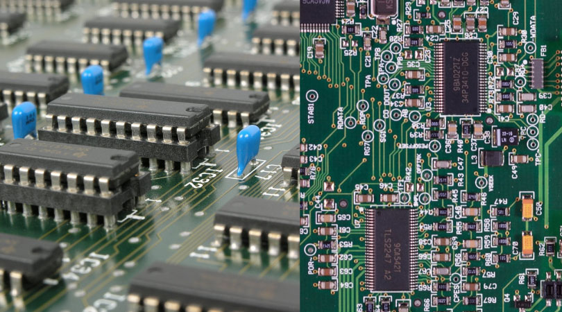
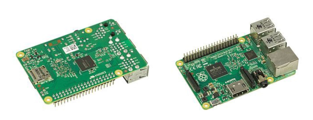
The easiest way to reduce the size of your circuit is by replacing the components with its smaller counterpart. If you are using through-hole components you can switch to SMD components. If you are already using SMD, you can use a smaller footprint.

Reduce Inter-component Spacing
Reducing the space between the components while placing the components on PCB will have a significant impact on the overall size. On the other hand, you should not compromise with min. clearance spec, this might impact high voltage circuits or will make your circuit difficult to solder or repair.

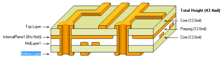
Increase PCB Layers
You need space on the PCB to route the tracks from one component to another and when you have more layers you get more space for routing. For example, if the board is of two layers, you can switch to 4 layers and easily reduce the size of the board as now you can route your signal quite easily and shift power /ground place to the inner layers. Now power and ground tracks will not interfere with the signal traces.

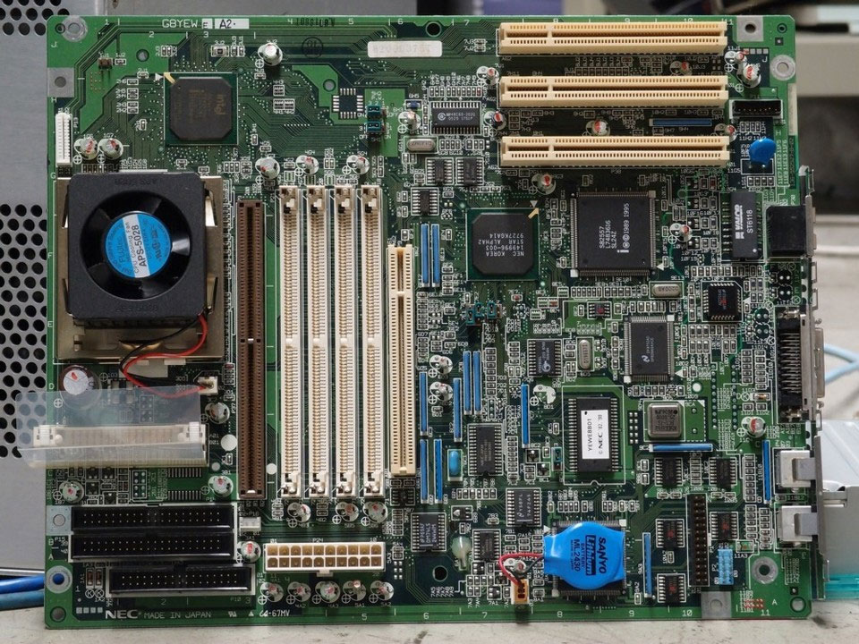
Both side component mounting
Often times, in order to keep the manufacturing challenges and cost low, designers choose to make PCBs with components mounted only on one side. In case you are can handle little more effort and cost of manufacturing due to component mounted on both sides of the PCB, this option greatly helps reduce the size of the overall PCB.

Integrated chips or modules
Think about a way to reduce the number of components on your board. Can you combine a few parts with a chip having more features integrated?
Some examples are:
- MCU with an integrated RTC
- Miniature power supply module instead of making one with discrete components
- BLE/WiFi combo module
- Chips with integrated ESD and other protection instead of using discrete
- RS232 / RS485 transceiver with isolation and protections inbuilt
- Use of driver chips instead of using a transistor and resistor based discrete driver circuit
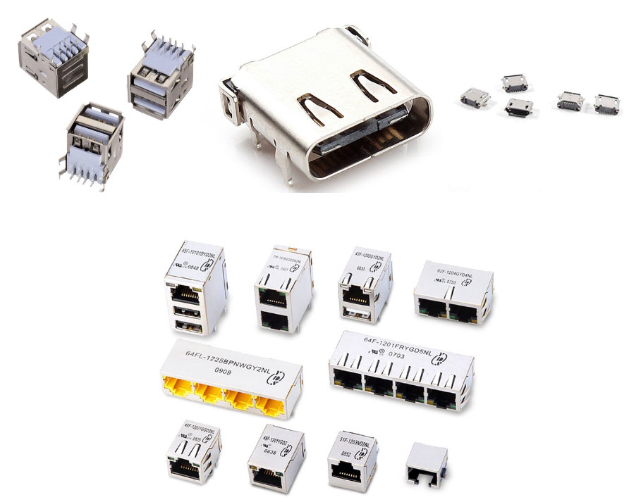
Review Connectors
In general, connector takes a significant part of the PCB space, review all connectors used and see if there is a smaller alternate or you want to combine few connectors together with a combo?

Optimize Flexibility
While designing a circuit, every designer keeps some flexibility in mind to handle EOL of a component, fall back options, uncertain behavior of a chip or circuit, easy of the test (test points) in mind and keeps those options on the circuit. Once the design is proven you can remove such options and reduce the overall circuit size.
Split the design
Some times to reduce the size, it becomes mandatory to split the design into two to more board and then connect them (piggyback) via appropriate connectors or cables. Need to be aware of the need for a special board to board connectors or cables, or mounting option, etc.


Reduce the overall design, think out of the box
Sometimes you need to think about the way you have designed the circuit, like, is there a way to reduce the overall complexity or circuitry?
some examples could be:
- In case your existing design, input power is from AC to 24V adapter and then in your circuit, you are using a DC-DC converter + heat-sink to make it compatible with 5/3.3V chips. Can you change to AC to 5V adapter and use LDO/DC-DC with reduced heat-sink, power section?
- In case you have multiple power rails(5V/3.3V/1.8V) in the circuit, is there a way to reduce those to fewer power rails?
- Sometimes using multiple capacitor values instead of one big value gives you more space.
- It might be possible to remove all the connectivity interfaces/connector like if you have RS232 & USB connector to connect your device to PC, you may want to explore an option for WiFi/BLE connectivity.
- Remove all heatsink and use the metal enclosure to dissipate all the heat by touching all chips to the enclosure using thermal pads.
Redesign
You might need to re-architect and redesign in some cases, no other way.
Common Challenges
There are various common challenges which might come while attempting to reduce the size of the design which one needs to be aware of, are as mentioned below:
- Soldering: Make sure you are aware of soldering challenges with smaller components. Hand soldering is going to be difficult with SMD component like in case you want to replace 0805 passives to 0603/0402 size. You might need to hire a more skilled soldering person or even go for machine solderings like in case you are replacing DIP/SOIC package chips to QFN packages or other lead-less packages.
- The cost could be a factor. When choosing a different package make sure you have noted the cost difference. Sometimes cost gets offset with the space-saving benefit it gives, example with smaller board your PCB cost might reduce, your packaging/shipping cost might reduce. So, consider the overall impact.
- Lead time is another constraint you must be careful about as many times these smaller footprint components have longer lead times.
- Component Spec: Be careful while replacing components(especially power components), with smaller footprint parts power handling capability reduces if you miss this critical parameter, you might face reliability issues in the field. Don’t compromise on the component spec or make sure you are aware of the impact while making the decision of changing the spec.
- Thermal Compatibility: While working on reducing the size of your design, make sure you have considered how the heat produced from different components will be handled, how it will affect other nearby components and affect the overall circuit’s performance. Often time we ignore this parameter and end up with a design with thermal issues.
- EOL / Alternates: It is always good to select a component whose replacement part is also available. While reducing the size of the PCB you might end up choosing a part where an alternate part might not be available, need to be aware of this risk.
- Testing Time & Effort: You might end up increasing the testing effort or difficulty with reduced size, so consider this important parameter.
- Increased Production effort: Make sure you have considered the impact you will have on your production effort and cost because of your reduced design’s size.
Do you know more ways, please do share in the comments section?