


“Synthesis” according to me is a crucial stage in the overall ASIC design process, where we can influence the course of the Chip Design process by doing a hell lot of fundamental Innovations which can benefit the next stages in the Backend cycle like Physical Design/Physical Verification/STA/Formality/Power Signoff etc. Looks confusing right? Don’t worry we will explore the synthesis world in detail and learn some proven techniques which I learned over many years working in some of the Complex Chips and Thanks to my companies who have given me the opportunities to Learn in my Career as a VLSI engineer. I would recommend both Front end/Back end engineers to continue reading the article since this is one skill that “looks good on a resume” for any VLSI engineer ( RTL/STA/PD/DFT etc)
Why do we need to synthesize the RTL? Because the real world does not work on if/else or case statements, Ultimately we need to break down the Specifications into Architectural Level/Logic Level/Gate Level stages and the Device needs to be Fabricated.
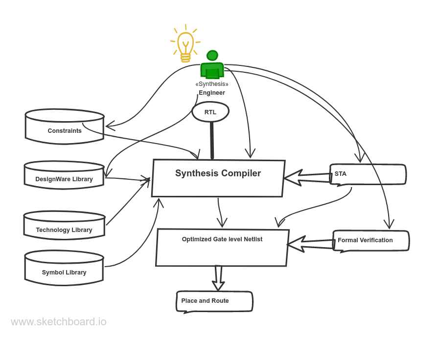
The main job responsibilities of a Synthesis engineer

- Checking the library consistency and Design consistency.
- Validating SDC constraints.
- Utilizing the Tool variables to get the desired end results.
- How to solve the Logic Level Optimization issues.
- How to solve Gate Level Optimization issues.
- How to know the DEF quality provided by Place&Route Engineer is Good enough.
- Gate count comparison w.r.t project specifications.
- Basic knowledge of DFT techniques.
- Complex topics
Wait for a second, Are you still reading? Okay Great! Please grab a cup of Coffee since the next discussion will be more technical related and how to approach the Problem to get workable solutions. Let’s dig into more details on each responsibility.
Checking the library consistency and Design consistency.
Before you start compiling you need to do few sanity checks like whether our desired inputs to Synthesis are proper or not for example any issues in the libraries provided to the Compiler and any issues related to RTL which will get caught in the Elaboration stage for example any linking issues are present then the Compiler immediately aborts the run. we use check_library and check_design commands to ensure the sanity check is done.
Validating SDC constraints
“SDC constraints step” is the “heart” of any Design synthesis effort. Wrong constraints result in bad results which if it gets caught very late in the design cycle is a sure shot disaster for the company and if proper care is taken initially can save a hell lot of money for the clients. I use the check_timing command to ensure I clean up the constraints before proceeding to the compilation step.
Right now in the market, we have some excellent constraint checker tools like TimeVision, Excellicon, etc which gives us more debugging capabilities to catch a lot of issues before even synthesis is mandatory to be completed. I pick up the RTL files, constraints then elaborate the design and check the constraints quality. Overall it just takes 15mins even for million gate count blocks as well, Unbelievable right!
Utilizing the Tool variables to get Desired End results
Each tool has a set of compile directives to ensure the tool works as hard as possible. I worked on two commercial tools namely Design Compiler and Genus. I would suggest exploring the timing optimization related variables on how to set them to High/Medium/Low based on the Design issues. ( Go to Solvnet/Cadence support websites)
Some of the variables which I regularly use to converge the synthesis timing is timing_effort_high/TNS_effort_high/Mux_mapping_effort_true/Better sequential Mapping/register_replication variables.
How to solve the Logic Level Optimization issues
To get the best Logic Level optimization I try to explore options like Flattening/Structuring/Ungrouping/Adaptive Retiming etc
Below is a one-line explanation of all the above techniques. For more details, I suggest you download Design Compiler and Genus Compiler User Guides.
Flattening
This helps in getting the best possible sum of product boolean expression on the design which I work on. Basically to reduce the levels of logic between two registers. This technique is used during the unmapped stage don’t forget ( precompile)
Structuring
Using temporary variables and reusing the same expression in the Boolean optimization can reduce a lot of operators ( adders/subtracters etc) and indeed reduce our overall Combinational logic between the registers. This technique is used during the unmapped stage don’t forget ( precompile)
Ungrouping
Too many hierarchies in the Design won’t allow the Compiler to come up with the best timing results, in this case, ungrouping comes in handy for the Engineer where we can merge sub modules to allow the compiler to do best boundary optimization to give quality synthesis netlist in terms of PPA ( power performance area). Beware of the optimizations since too many optimizations can cause issues for DFT insertion and also Formal verification can be tough. Use this technique wisely.
Adaptive Retiming
Retiming is the movement of registers back and forth between combo logic. So how do we come up with the idea of applying retiming on the Design? Basically, I try to see the margins on the start point flop data pin and endpoint flop output pin and check the timing path in Layout, since in DEF based synthesis we have the luxury of opening Physical layout for visual analysis.
How to solve Gate Level Optimization issues
Gate level optimization is more of local optimization, If we use physical synthesis try to apply path_groups, Low threshold cells, and placement_bounds, etc to see if you can see any improvement in timing results. Blind application of path groups and placement bounds in synthesis won’t work. Multibit registers are also one technique to reduce power consumption. Quad flops, Octa flops are usually seen in SOC’s designed today to save power.
“Always ensure first to root cause the issue and later apply these techniques.”
How to know the DEF quality provided by Place&Route Engineer is Good enough.
Synthesis engineers should also be equally responsible for catching any bad Macro placement in the Design, But how is it possible since I don’t know Innovus or ICC2?
See I already discussed this previously, Physical aware synthesis has the feature to support opening Layout for visual data connectivity analysis and see the module splitting issues once we start debugging it would be easy to catch any bad Macro placements coming from the DEF and based on the final conclusion we can provide the same feedback to PD engineer to rework on the DEF placements. Based on my past experience I can say bad Macro placement has resulted in a huge increase in Buffer/Inverter counts excluding the normal combo gate counts. Imagine the amount of power and congestion we can solve just doing proper compiling!! Sounds amazing to me 🙂
Gate count comparison w.r.t project specifications.
Combinational Gate count is the amount of combinational cell area excluding flop area, memory area, and black box areas (if present) divided by smallest drive strength 2 input NAND gate area for a particular technology node. This may not be of much interest to everyone since this is more of finance rather than technical, Anyway, let me explain why combinational gate count matters!. Usually, flop count and memory count are kind of standard for any project to project but when a vendor wants to negotiate and wants to come up with Chip Area ( Silicon area) they come up with some estimation and plan the partitions in the Chip based on the logic and application complexity. They call it RFQ ( Request for Quote). If the synthesized netlist is too far from RFQ numbers then we are in trouble. It might give us a clue like we might need to increase the silicon area or not. Remember we can afford to lose 1-acre land in Silicon Valley however we can’t afford to lose 1mm silicon area in Wafer which is even more costly 🙂
Basic knowledge of DFT techniques.
Since scan insertion happens in synthesis, a Basic idea of DFT is required for any engineer. Scan coverage, fault coverage reports will give us some basic idea of the DFT quality for a block. Based on the results we can discuss them with DFT teams.
Complex topics
Anything which I don’t understand or never worked I usually put in the complex topics category. Pun intended !! If you are getting hired usually clients won’t expect you to work only in synthesis, sometimes they require engineers who handle Formal verification and STA aspects as well along with Synthesis which is beyond the scope of this article. As the design complexity increases and clocks in the SOC increase in the future, even backend engineers would play a crucial role in CDC ( clock domain crossing). Oh my God, there are so many things that I need to learn to stay relevant in the industry and match the future requirements of my Clients. Thanks a lot, friends for patiently reading, we are done for now 🙂 🙂
By Sriharsha Pudi, STA engineer @spicaworks