

By Shital Joshi, Synopsys
Packaging is something that is often viewed as the final stage between chip fabrication and the finished product. That perception is changing quickly.

Packaging is increasingly becoming a critical part of system-level innovation with semiconductor architectures evolving toward chiplets, heterogeneous integration, 2.5D and 3D architectures, and high-bandwidth memory (HBM). The package is no longer only protecting the silicon, it is also helping determine performance, power efficiency, thermal behaviour, reliability and, ultimately, the competitiveness of the product.

This shift is particularly significant for Outsourced Semiconductor Assembly and Test (OSAT) providers as their role is expanding from executing highly specialised assembly and test processes to becoming important innovation partners for semiconductor companies.
This evolution comes with a fundamental engineering challenge: how can OSATs manage increasing package complexity while improving yield, reliability and time-to-market?
The answer is: engineering that is simulation-driven.
Physical Experimentation to Virtual Engineering
Advanced semiconductor packaging connects materials and processes with very different physical characteristics. Thin copper interconnects, organic substrates, silicon dies, underfills, mold compounds and solder structures – all respond differently to temperature, mechanical loading and manufacturing processes.
Relatively small variations can translate into significant reliability problems as package dimensions shrink and integration density increases. Warpage, die cracking, solder fatigue, delamination, void formation and other failure mechanisms can arise from interactions between materials and manufacturing steps.
And since these effects do not occur in isolation, it is a challenge.
Residual stress can be created by a process step, which then influences the next stage of assembly. Thermal cycling can change mechanical behaviour. Changes in material properties can disturb warpage and reliability. A package that performs well in one simulation domain can still encounter problems when thermal, mechanical and electrical effects interact.
This is why physics-based simulation is increasingly valuable. Engineers can use simulation to understand how a design or manufacturing process is likely to behave before committing to expensive production experiments. They do not have to rely exclusively on physical builds to discover problems. The objective is not to completely eliminate physical validation, but to make every physical experiment more targeted and informative.
This can change the economics and speed of engineering.
Simulation across the OSAT Value Chain
Consider the journey of an advanced semiconductor package.
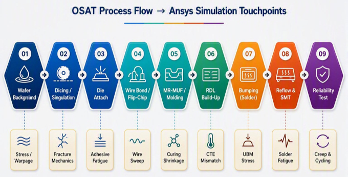
Reducing silicon thickness can introduce stress and subsurface damage during wafer backgrinding. Understanding the relationship between process parameters, material properties and structural integrity becomes increasingly important when dies become thinner.
Mechanical, laser or plasma processes can introduce chipping or initiate microcracks during dicing and singulation. Simulation can help engineers study stress concentrations and fracture behaviour, thus allowing process parameters to be evaluated before production.
Die attach comes with another set of challenges. Adhesives and sintered materials shrink during curing and create stresses at interfaces. Understanding these stresses helps engineers evaluate material choices and process conditions.
Flip-chip assembly also has complexities. Microbumps, under-bump metallisation and redistribution layers must be able to withstand thermal excursions and mechanical loading. Reliability cannot be treated as an afterthought at these dimensions.
The same applies to molded underfill processes. In mass reflow with molded underfill (MR-MUF), for example, flow behaviour, void formation, filler distribution and subsequent warpage can all influence package quality.
Multiple material layers with different coefficients of thermal expansion can accumulate stress during deposition and curing in the RDL build-up. Another challenge. Predicting the resulting deformation can help engineers understand warpage and potential line-break risks before manufacturing.
Also, board-level assembly subjects packages to reflow, thermal cycling, vibration and other operational stresses. Reliability simulation can help connect package-level decisions to expected field performance.
Simulation’s value therefore increases when it is applied across the process chain rather than when used as an isolated design exercise – from wafer thinning and singulation through RDL, reflow and board-level reliability.

The Rise of Multiphysics Packaging
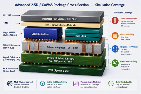
One more change is that packaging problems are increasingly becoming multiphysics problems. Consider HBM and advanced 3D integration. Putting multiple dies and high-density interconnects into a compact package can deliver enormous improvements in bandwidth and computing performance. However, concentrating more functionality and power into a smaller physical space also creates thermal and mechanical challenges.
A thermal problem can become a reliability problem. An electrical design decision can influence power density and heat generation. Mechanical deformation can affect interconnect integrity. In short, the different engineering domains are becoming increasingly interconnected.
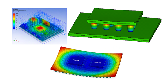
This challenge is very much present in multiphysics modelling of HBM and 3D heterogeneous integration, where high power density and localised hotspots can create thermal, mechanical and reliability concerns. This is why advanced packaging requires engineers to move beyond analysing individual phenomena independently.
Thermal analysis, structural mechanics, computational fluid dynamics and electromagnetic simulation increasingly need to work together to provide a more complete picture of package behaviour.
So the need of the hour is Mechanical for structural and thermomechanical analysis, Icepak for thermal analysis, Fluent for fluid and process simulation, HFSS and related electromagnetic technologies for signal and power integrity, and Sherlock for electronics reliability. These simulation domains work across packaging and board-level applications.

Making Reliability Part of the Design Conversation
Traditionally, reliability qualification can involve multiple physical iterations. If a failure is discovered late in the development process, changing the package design or process can be expensive and time-consuming.
One of the most important opportunities for OSATs is to move reliability further upstream and simulation allows reliability considerations to become part of earlier engineering decisions.
For example, engineers can evaluate different materials, package configurations, thermal conditions or process parameters virtually and identify potential weaknesses before committing to a large number of physical builds.
This can also strengthen collaboration between OSATs and their semiconductor customers. An OSAT that can provide insight into package reliability, thermal performance and manufacturing sensitivity early in the development cycle is contributing more than manufacturing capacity as it is contributing engineering intelligence.
This is becoming increasingly important as semiconductor companies develop products for artificial intelligence, high-performance computing, automotive and other demanding applications.
Advanced packaging shows how simulation is already being applied to these challenges. Simulation solutions have been certified for advanced packaging technologies including TSMC’s CoWoS and InFO technologies and Samsung’s multi-die packaging technologies, supporting analysis across thermal, power, signal and reliability domains.
From Simulation to Optimisation
The real opportunity goes beyond simply running simulations. Modern simulation can be used to explore large numbers of design and process combinations. Design-of-experiments and optimisation techniques can help engineers identify which parameters have the greatest influence on performance and reliability.
This creates the possibility of defining wider and more robust process windows rather than optimising a process around a single nominal condition. For OSATs, that can have significant business implications: faster qualification, improved yield, fewer iterations and greater confidence when introducing new materials or packaging technologies.
It also creates an opportunity to reduce waste. Every failed physical build consumes materials, energy, engineering resources and production capacity. Using simulation to narrow down the most promising options before physical validation can help reduce unnecessary iterations.
The goal is to make engineering decisions more informed and not simply to make engineering faster.

Towards the Digital OSAT
In future, simulation will become increasingly integrated with manufacturing data. The next generation of OSAT operations will combine simulation, process data, metrology and artificial intelligence to create more adaptive engineering workflows.
Imagine a manufacturing environment where package warpage, temperature, material variation and other process measurements continuously feed calibrated simulation models. Instead of responding to defects after they occur, engineers could identify emerging patterns and adjust process conditions proactively. This is the foundation of the digital twin concept for semiconductor packaging.
AI can further accelerate this transformation by creating surrogate models that approximate complex physics much faster, enabling engineers to explore more design and process possibilities.
With advanced AI-enabled simulation capabilities, including SimAI, there is also a broader movement toward combining physics-based engineering with machine learning. AI-augmented simulation, digital twins and system-technology co-optimisation are important emerging frontiers for the industry.
The ultimate opportunity is system-technology co-optimisation. As the boundaries between chip design, package design and system design continue to blur, decisions about die architecture, bump placement, RDL routing, interposer design, thermal management and board implementation cannot be made independently.
Simulation provides a common engineering framework through which these trade-offs can be evaluated.
Building the Next Generation of OSAT Competitiveness
The OSAT industry is entering an important new phase. Advanced packaging is becoming a critical enabler for AI, HPC, automotive and other compute-intensive applications. At the same time, package architectures are becoming more complex, development cycles are under pressure and reliability expectations are increasing.
In this environment, manufacturing excellence alone will not be enough. The OSATs that differentiate themselves will be those that combine manufacturing expertise with deep engineering capabilities, and simulation will be a key part of that capability.
The shift is therefore from reactive problem solving to predictive engineering and not simply from physical testing to virtual testing.
Simulation allows engineers to ask “what if?” earlier, evaluate more alternatives, understand failure mechanisms more deeply and make physical experimentation more purposeful.
As advanced packaging moves toward finer pitches, thinner structures, higher power densities, new materials, hybrid bonding and increasingly complex chiplet architectures, that capability will become even more important.
For the semiconductor industry, the future of packaging will be defined by how confidently it can be designed, manufactured and qualified. It will not only be about how small or sophisticated a package can become. Simulation-driven engineering can help make that confidence possible.
The next generation of OSAT innovation will be engineered first in the virtual world, and then validated in the physical one.