
Spintronics AI Evaluates Potential Site for Proposed GaN Semiconductor Fabrication Facility in Ujjain, Madhya Pradesh with Proposed 2800cr investment
Following an invitation from the Madhya Pradesh Government, the company’s team visited Vikram Udyogapuri, Ujjain, to assess the site’s suitability for a proposed semiconductor manufacturing facility.
India, 27th October 2026: Spintronics AI Semiconductors, a Hyderabad-based semiconductor design and product engineering company working across Gallium Nitride (GaN), RF, power semiconductors and power-management technologies, is evaluating the feasibility of establishing a GaN semiconductor fabrication facility in Madhya Pradesh.
As part of ongoing discussions, the Government of Madhya Pradesh invited the company to evaluate a land parcel at Vikram Udyogapuri in Ujjain. The Spintronics AI team subsequently visited the location and shared its initial observations with the Government.

Spintronics AI and its technical and industry expert panel are assessing the site against key requirements for semiconductor fabrication, including air quality and environmental conditions, water availability and quality, reliable power infrastructure, utilities, cleanroom requirements, logistics, waste management, supporting infrastructure and overall site suitability.
An overall land requirement of approximately 40 acres is being considered, with around 24 acres envisaged for Phase I and the remaining land planned for subsequent phases. The proposed land requirement and project configuration remain subject to detailed feasibility assessments and project needs.
Subject to the outcomes of feasibility assessments, necessary approvals, applicable incentives and project structuring, Spintronics AI is considering an overall investment programme of approximately ₹2800 crore for the proposed semiconductor initiative.
The current indicative plan envisages an investment of up to ₹800 crore in Phase I, followed by subsequent expansion phases based on technology readiness, market demand, infrastructure development and commercial requirements. These figures represent a preliminary investment roadmap and are not a final investment commitment to the proposed Ujjain facility.
At full development, the proposed project could support up to 1,000 direct and approximately 2,800 indirect employment opportunities across semiconductor engineering, manufacturing, equipment, infrastructure, supply chains and supporting industries. These preliminary, long-term projections will depend on the final project scope and phased implementation.
Raghu Varma, Founder & CEO, SpintronicsAI Semiconductors, said, “Madhya Pradesh’s push to bring the technology of the future to the state gives us the opportunity to build capability in stages, with design and engineering strength in Indore and GaN technology development in Ujjain reinforcing each other. We want every stage to be earned through sound technical and environmental assessment, so that what we eventually build in India is commercially viable and built to last.”
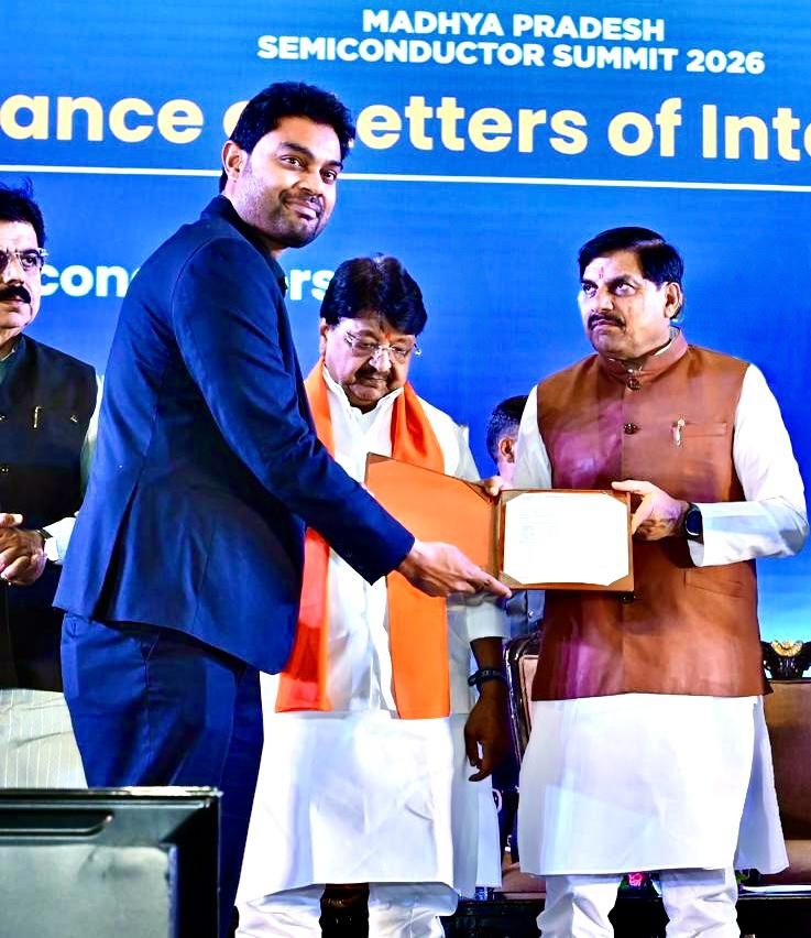
Following discussions with Hon’ble Chief Minister Dr Mohan Yadav, the Government of Madhya Pradesh issued a Letter of Intent (LOI) to Spintronics AI, reflecting its interest in facilitating the company’s semiconductor research and development (R&D), design and product engineering activities in the State. The proposed support includes suitable space and ecosystem assistance for an early-stage presence.
Separately, Spintronics AI is exploring GaN technology development in collaboration with CSIR-Central Electronics Engineering Research Institute (CSIR-CEERI), Pilani. This work forms part of the company’s broader efforts to assess pathways for indigenous GaN technology development and potential domestic manufacturing.
The proposed Ujjain facility remains under preliminary feasibility evaluation. The findings will inform the company’s next steps, with any final investment decision and implementation timeline dependent on the technical, commercial, environmental and infrastructure assessments, project requirements and necessary approvals.