

Singapore, September 25, 2025 – ASMPT, the global leader in advanced packaging and assembly solutions, and KOKUSAI ELECTRIC CORPORATION, a pioneer in front-end semiconductor equipment, announced a Joint Development Agreement (JDA) to collaboratively advance hybrid bonding (HB) and micro-bump thermo-compression bonding (TCB) technologies. This strategic partnership is set to deliver more robust solutions to accelerate the adoption of 2.5D and 3D heterogeneous integration and empower the next wave of High-performance Computing (HPC) and Artificial Intelligence (AI) applications.
This JDA combines KOKUSAI ELECTRIC’s sophisticated thin-film technology with ASMPT’s ultra-high-precision bonding technology to deliver more robust HB and micro-bump TCB solutions that will lead to more effective solutions for advanced 2.5D and 3D packaging, with improved product quality, yield, and accelerated time-to-market for high-performance, energy-efficient chips.

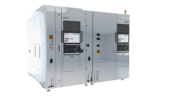
“By integrating our state-of-the-art thin-film technology with ASMPT’s precision bonding platforms, we are addressing critical advanced packaging process challenges and setting new industry benchmarks for both hybrid bonding and thermo-compression bonding,” explained Hidehiro Yanagawa, Executive VP of KOKUSAI ELECTRIC CORPORATION. “Our partnership with KOKUSAI ELECTRIC will truly push the boundaries of advanced packaging technology,” remarked Nelson Fan, VP of ASMPT SEMI Solutions’ AP Business Group. “Through this close collaboration, we are looking forward to unlocking further possibilities with our patented AOR TCB™ (the process with our FIREBIRD bonder), and our cutting-edge LITHOBOLT® hybrid bonding platform, to deliver robust, scalable, and high-quality solutions for the future.”

This alliance positions both companies as leaders in semiconductor packaging innovation for next-generation computing technologies.