

Introduction
The CD4066 is a CMOS integrated circuit that contains four independent bilateral switches. These switches can pass both analog and digital signals in either direction, making the IC highly versatile for signal switching applications. The term Quad Bilateral Switch means that the IC contains four electronically controlled switches, each capable of conducting signals in both directions when activated.
Pin Configuration of CD4066
| Pin Number | Pin Name | Description |
|---|---|---|
| 1, 4, 8, 11 | IN/OUT SIG A, B, C, D | Input/Output terminals for Switches A, B, C and D |
| 2, 3, 9, 10 | OUT/IN SIG A, B, C, D | Output/Input terminals for Switches A, B, C and D |
| 5 | CONTROL B | Control input for Switch B |
| 6 | CONTROL C | Control input for Switch C |
| 7 | VSS | Ground terminal of the circuit |
| 12 | CONTROL D | Control input for Switch D |
| 13 | CONTROL A | Control input for Switch A |
| 14 | VDD | Positive supply voltage |
Working of CD4066 Quad Bilateral Switch
The CD4066 consists of four independent electronic switches controlled by digital logic signals. Each switch has:


- Two signal terminals
- One control terminal
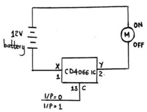


When a HIGH logic signal is applied to the control input, the corresponding switch turns ON and allows the signal to pass between its two terminals. When a LOW logic signal is applied to the control input, the switch turns OFF and blocks signal transmission. Since the switches are bilateral, signals can flow in either direction through the switch when it is ON.
Features of CD4066
- Four independent bilateral switches in a single IC
- Can switch both analog and digital signals
- Low power consumption
- Wide operating voltage range
- High noise immunity
- Simple control using logic signals
- Bidirectional signal flow capability
Advantages of CD4066
- Easy to interface with digital circuits
- Suitable for analog signal switching
- Compact design with four switches in one package
- Low ON resistance
- Reliable operation
Applications of CD4066
- Analog signal multiplexing
- Digital signal switching
- Audio signal routing
- Sample and hold circuits
- Communication systems
- Data acquisition systems
- Electronic instrumentation
- Automatic control circuits
Conclusion
The CD4066 Quad Bilateral Switch is a versatile CMOS integrated circuit containing four independently controlled bilateral switches. Its ability to switch both analog and digital signals in either direction makes it widely useful in communication, audio, instrumentation, and signal processing applications.