A properly doped PN junction diode, which has a sharp breakdown, is known as a zener diode. It is also called a voltage reference, voltage regulator or breakdown diode. The zener diodes are silicon PN junction devices which differ from rectifier diodes in the sense, they are operated in the reverse breakdown region and the breakdown voltage is set by carefully controlling the doping level during manufacturing process. Thus, by controlling the junction width and doping concentration of PN junction diode, it is possible to make it to breakdown at a sharp specified zener voltage.
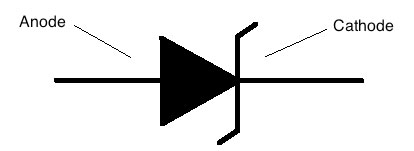
A zener diode is represented by a schematic symbol as shown in below figure. It has two terminals namely, anode and cathode. As memory aid, it may be noted that at the end of the arrow looks like the letter Z.