


Based on the wide bandgap (WBG) material gallium nitride (GaN), new power switches deliver superior efficiency and enable higher switching frequencies, opening up a new era in power electronics. To support this development, Infineon Technologies AG announcedd uring PCIM Conference 4 – 6 May 2021 a new family of CoolGAN™ IPS integrated power stage (IPS) products to its broad portfolio launched.
To learn more about this GaN products and this launch, SemiconductorForU spoke to Thomas Beer, Senior Director Strategic System Application Engineering CoolGAN™ (Power & Sensor Systems division), Infineon.
Background, why GaN HEMT and WBG Wide Band Gap semiconductors?
All electronic devices that we use today have components inside made of semiconductors, mostly silicon. In recent years, gallium nitride (GaN) known already in the market of high RF Radio Frequency designs, is another semiconductor, which is making its way into power electronics as its device characteristics (often called FoM´s Figure Of Merits)are better suited for high power and high-frequency applications, compared to silicon MOSFETs. Since GaN as a power-technology is still evolving, and it is less expensive to set up a foundry for manufacturing, it is touted to be one of India’s opportunity to mark its presence in the niche field of semiconductors. An interdisciplinary group of faculty members at IISc have also researched and developed India’s first-ever e-mode gallium nitride power transistor, whose performance is comparable to some of the best reported till date.
This new type of power transistors are also called High Electron Mobility Transistors or HEMTs. These transistors are made with gallium nitride, and they can operate at very high voltages, switch ON and OFF faster, and occupy less space when compared to silicon-based transistors.


Tell us more about Infineon’s e-mode GaN HEMT?

A High Electron Mobility Transistor (GaN HEMT) has a lateral conducting channel between two terminals, source and drain, and the current through the channel is controlled by a third terminal called gate.
GaN-based devices are available as “normally-on” or depletion mode (d-mode) HEMTs or as e-mode GaN HEMT, where the conducting channel is in “normally-off” mode if no gate signal is applied or no auxiliary supply gate drive voltage is present in the system (e.g. if the full system is unpowered). This is also called “normally off” GaN HEMT or enhancement mode (e-mode) HEMT.
For he d-mode transistors there are various techniques to achieve a normally-off state. One such approach is to completely recess of the channel—which results in reducing the channel size. Another method is to additional added a lower voltage cascode switch transistor to keep the channel normally-off. However, these methods can affect the stability, performance and reliability of the device during operation and lead to abnormal conditions compared to a true e-mode normally off transistor.
Another approach is to use a gate made in the gallium nitride, doped with impurities that deplete electrons from the channels where the switch is default in normally-OFF mode, which is accomplished via the p-Gate structure. The challenge with this method is that the gate and the channel form a parasiticdiode, which starts conducting current when a voltage greater than a certain GaN HEMT threshold value is applied at the gate. However, the advantage of the p-Gate isan easy to drive gate with higher stability of the gate andno need for Zener diodes to protect the gate against over-voltages.Further the p-Gate delivers a better dynamic RDSonover temperature.
What is the key Figure of Merits FoMin the high voltage 600V discrete & IPS- CoolGaN™?
Compared to silicon (Si), the breakdown field of Infineon’s CoolGaN™ enhancement mode (e-mode) HEMTs is ten times higher and the electron mobility is double. Both the output charge and gate charge are ten times lower than with Si and the Qrrreverse recovery charge is almost zero which is key for achieving less switching losses in a half-bridge operation. The low Qrr is also the key enabler in hard switching topologies, and enables the Totem Pole PFC for medium to high power conversion.
Please note, a GaN HEMT has not a “hard” breakdown voltage at 600V, compared to a silicon power MOSFET which hasan avalanche effect and would destroy at short term over-voltages. All CoolGaN™ power devices are JEDEC tested with 750V and more than 10 Mill cycles of short term (transient) impulses (as outlined in our datasheets).
GaN is the suitable technology of choice in hard switching as well as resonant topologies, and is enabling new approaches in current modulation. Infineon’s discrete and IPS CoolGaN™ can be flexible choice in the system partitioning across many applications from low to high power such as USB-PD charger, server-telecom SMPS, wireless charging, adapter and audio.
What benefits do we get with the CoolGaN half-bridge launched in PCIM Virtual event?
Infineon Technologies has expanded its well established GaN-based discrete product portfolio and package options with the introduction of the new CoolGaN IPS family. The initial portfolio of integrated power stages consists of both half-bridge and single-channel products, targeting low-to medium power applications, including USB-PD (PD power delivery) standard compliant chargers and adapters and low to medium power switched-mode power supplies (SMPS).
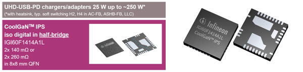

The 600V CoolGaN half-bridge IPS IGI60F1414A1L targets compact and lightweight designs in the low-to-medium power range. Housed in a thermally enhanced 8 × 8 QFN-28 package, the IPS combines two 140 mΩ/600 V CoolGaN e-mode HEMT switches with dedicated galvanically isolated high- and low-side EiceDRIVER gate drivers.
The IGI60F1414A1L is easy to control due to the isolated gate driver with two digital PWM inputs. The integrated isolation function, the clean separation of digital and power ground and the reduced complexity of the PCB layout are crucial in achieving shorter development time, lower system bill-of-material and lower total cost. The gate driver’s input-to-output isolation is based on Infineon’s proven on-chip coreless transformer (CT) technology. This guarantees high speed and excellent robustness utilizing the GaN with its extremely fast switching slew rates with voltage slopes exceeding 150 V/ns.
(e.g. 3*150V/ns = you need 3ns to reach 450V bus voltage in the system)
The switching behavior of IGI60F1414A1L can be easily adapted or slowed down to the needs of different applications by means of a few passive gate path components. This allows slew rate optimization for example to reduce electromagnetic interference (EMI) efforts, steady-state gate current setting, and negative gate drive for fast turn-off and robust operation in hard-switched applications.
Furthermore, due to the system-in-package integration and the highly accurate and stable propagation delay of the gate drivers, the IGI60F1414A1L enables the lowest possible system dead-times. This helps to maximize system efficiency, leading to the next level of power density up to 35 W/in³ for charger and adapter solutions. Flexible, easy and fast designs are also enabled for other applications, including LLC resonant topology and motor drives.
What are the advantage of Infineon`s single channel CoolGaN™ IPS and its embedded isolated gate driver – EiceDRIVER™ technology?
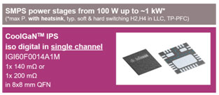

Thesingle CoolGaN™-IPS IGI60F0014A1M has for switching speed and performance the same GaN and embedded functional isolated EiceDRIVER™ features as the half-bridge device for power-landing in the PCB design, however it will come in the future with lower RDSons and has about double the thermal capabilities of the package, as there is only one switch inside.
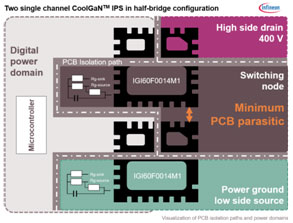

Further to the half-bridge device, the gate drive dv/dt slew rate control can now be individually configured and done with less PCB components than in the half-bridge configuration.
The package pin-out has been created to allow for a minimum distance (typ. creepage distance) side by side placement of the single-channels on the PCB as a half-bridge to create least parasitic switching node loop on the PCB.
How do you see the future of GAN Integrated power stages?
The higher circuit integration density for smaller PCB form-factors, the superior GaN HEMT lower loss switching characteristics combined with the simplicity to drive a GaN Power HEMT with basically any digital controller (GPIO) PWM signals, is what we see the markets demand today.
The GaN market will develop further and from Infineon you will see many more new advancements with the next generations of GaN HEMTs, as the integration density utilizing the lateral device functionality will increase and enable smarter, safer and higher integrated mid- and high voltage HEMTs.