

555 Timer IC is very popular IC and very useful in the timing related application. For example whenever it is used as a relaxation oscillator, then it can be used as a tone generator or the alarm generator and even it can be used for the frequency division or for generating the timing delays. 555 timer IC is available in so many packages.
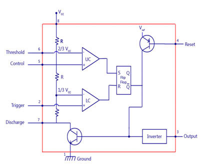


Above is the internal block diagram of 555 timer IC. Many blocks and components are used for 555 timer. The basic blocks of 555 timer IC are –

- Voltage divider circuit
- Comparators
- Flip-flop
- discharge circuit
- output driver circuit
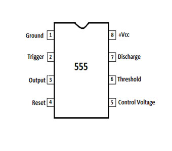
The purpose of pin number 1, 3 and 8 is pretty straightforward. In 555 timer IC, the pin number 8 is the supply voltage pin and usually, the supply voltage in the range of 4.5 to 15V is applied at this pin. Pin number 1 is the ground pin. It is connected to the circuit ground. The pin number 3 is the output pin. So, this pin is capable of driving the TTL loads and it can source or sink up to the 200mA of current.
The first block of this 555 timer IC is the voltage divider circuit. Now, we can see in the block diagram, the voltage at two modes are going to the comparator. Assume that the op-amp which is used as a comparator is an ideal op-amp. So, no current is flowing into the op-amp terminals. So, we can say that from this supply voltage, the current is flowing only through three resistors and that why we can direct apply the voltage divider rule. So, by applying the rule we can say that the voltage at the negative terminal of the first comparator is (2/3) Vcc. Similarly, the voltage at this node can be found using the voltage divider rule. So, the voltage at the positive terminal of 2nd node is (1/3)Vcc. The other two pins going to comparator are threshold and trigger pins. These two pins are input pins and by changing the voltage at these two pins, we can change the output of this comparator. The inverting node of this first comparator is at the 2/3 Vcc voltage. Whenever threshold voltage goes above this (2/3) Vcc voltage then, the output of the comparator will become high voltage and its similar for the trigger input. Trigger voltage used to be at the supply voltage and whenever we want to change the state of the comparator, then the trigger signal is changed in such a way that output at the pin number 2 goes below (1/3) Vcc voltage. When the output of comparator changes, then it will affect the other circuitry. The output of the comparator is given to the flip-flop circuit. The flip-flop used in 555 timer is the RS flip-flop.
TRUTH TABLE OF RS FLIP-FLOP
TRUTH TABLE OF RS FLIP-FLOPAs this RS flip-flop is a digital circuit, so the input of the flip-flop will be either logic 1 or logic 0. over here we are only interested in two condition that is when the input is 0 and 1. Let’s assume that the trigger signal is at Vcc voltage that is the output of the second comparator is at logic 0 or S=0. Now, let’s assume that threshold voltage is less than reference voltage, at that time the output of the first comparator will be equal to 0. So, the output of the flip-flop will remain same as it is now, whenever threshold voltage goes above (2/3) voltage, then the output of the first comparator will become logic 1. So, at that time the output of the flip-flop will be equal to 0. The output of the flip-flop is zero and because of that the output of 555 timer will also become zero. By threshold voltage, we are controlling the output voltage and same is true for trigger pin and in a way we are controlling the timing of output signal. To change the input voltage to threshold pin, the external resistor and capacitors are connected between threshold and the discharge pin through the supply voltage and same goes for trigger signal. There is one more pin, using which timing can be controlled and that is pin number 5. pin number 5 is known s the control pin and it is directly connected to the inverting terminal of the first comparator. By using control pin, external reference voltage can be applied and by which the timing of the output signal can be changed. Discharge pin helps the capacitor in the discharging whenever the output is in a low state. Last pin which is retained is the reset pin. Reset pin is an active low pin, it means that when logic 0 is applied to pin, then flip-flop of 555 timer will get reset and the output of the 555 timer will also get reset. So, irrespective of the working of 555 timer, whenever reset pin goes low, the the output will be zero volts.
In 555 timer IC, by changing the inputs we can control the timing of the output signal and by connecting the external components like a resistor and capacitor 555 timer can be configured either as astable, monostable and bistable multivibrator.
Truth table of RS flip
|
S |
R | Qn | Qn+1 |
| 0 | 0 | 0/1 | 0/1 |
| 0 | 1 | 0/1 | 0 |
| 1 | 0 | 0/1 | 1 |
| 1 | 1 | 0/1 | x |