


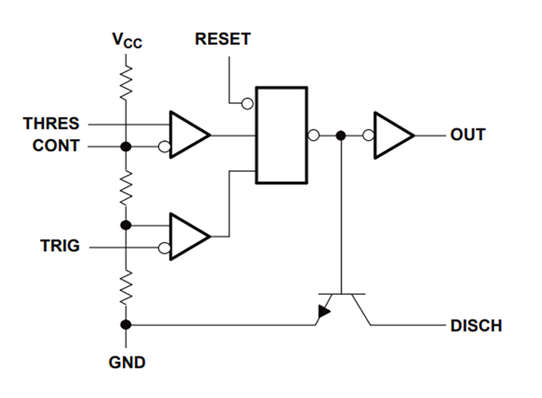
- The LM556 Dual timing circuit is a controller capable of producing accurate time delays or oscillation.
- The LM556 is a dual 555. Timing is provided by an external resistor and capacitor for each timing function. it has two timers that operate independently of each other sharing only VCC and ground. The circuits may be triggered and reset on falling waveforms.
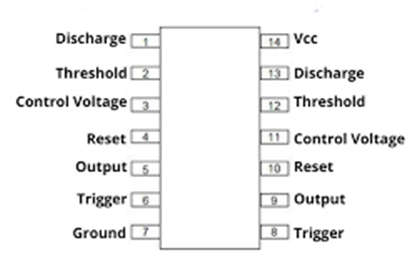
Pin Configuration


| Pin | Pin Name | Description |
|---|---|---|
| 1,13 | Discharge | Open collector output which discharges a capacitor between intervals (in phase with output). |
| 2,12 | Threshold | Compare the voltage applied to the terminal with a reference voltage of 2/3 Vcc. The 6 I amplitude of the voltage applied to this terminal is responsible for the set state of the flip-flop. |
| 3,11 | Control | Controls the threshold and trigger levels. An external voltage applied to this pin can also be used to modulate the output waveform. |
| 4,10 | Reset | A negative pulse is applied to this pin to disable or reset the timer. |
| 5,9 | Out | connected to load as it is the only pin with output-driven waveform. |
| 6,8 | Trigger | Responsible for the transition of the flip-flop from set to reset. |
| 7 | Ground | Ground Reference Voltage 0V. |
| 14 | Vcc | Supply Voltage (Typical = 5V, Maximum = 18V). |
Working
- There are two sets of all the timer pins (Threshold, Out, Trigger, Control Voltage, Discharge), and both the timer share the same Vcc and ground pins.
- Three resistors of value 5K, which gives this IC the iconic name “555 Timer”.
- It has dual comparators and flip-flops which will make this IC operate in three different modes such as Astable, Monostable, and Bistable(Schmitt) Mode.
- Timer ICs are the most commonly used ICs for timing and Pulse generation applications. They can adapt themselves to various applications due to their different operating modes.
Applications of LM556 Dual Timer IC
- Pulse Width Modulation
- Pulse generation
- Precision Timing
- Sequential Timing circuit
