

Shipments Increase in 2025 Amid Strong AI-driven Demand, While Revenue Softens
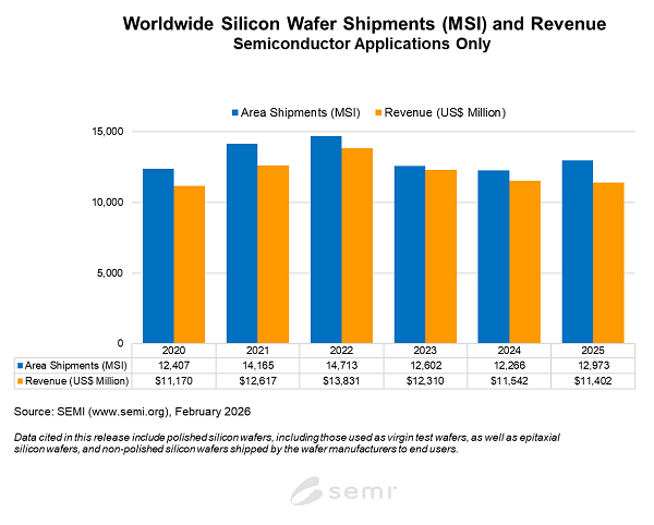
MILPITAS, Calif. — February 10, 2026 — Worldwide silicon wafer shipments in 2025 increased 5.8% to 12,973 million square inches (MSI) while wafer revenue slipped 1.2% to $11.4 billion over the same period, the SEMI Silicon Manufacturers Group (SMG) reported in its year-end analysis of the silicon wafer industry.
2025 marks an inflection year for wafer shipments, with silicon MSI resuming growth supported by strong demand for advanced epitaxial wafers in logic and polished wafers for high-bandwidth memory (HBM), driven by AI applications. Softness in wafer revenue is mostly attributed to the slow momentum in traditional semiconductor applications where the demand and pricing environment are yet to improve.
“The 2025–2026 wafer market is shaped by diverging trends across technology nodes,” said Ginji Yada, Chairman of SEMI SMG and Executive Office Deputy General Manager, Sales and Marketing Division at SUMCO Corporation. “Demand for 300mm wafers remains strong in advanced applications, particularly in AI-driven logic and high-bandwidth memory (HBM), supported by the ongoing adoption of sub-3nm processes. These technology transitions are driving increased requirements for wafer quality and consistency, reinforcing the need for advanced material solutions. Investments in data centers and generative AI continue to underpin demand in leading-edge segments, where performance and reliability are critical.

“In contrast, the legacy semiconductor segment shows gradual signs of stabilization. Wafer and chip inventory levels in mature-node applications—such as automotive, industrial, and consumer electronics—have begun to normalize after extended inventory adjustments. While supply-demand conditions are improving sequentially, the pace of recovery remains moderate, with demand recovery still sensitive to macroeconomic factors and end-market dynamics. As a result, the overall market outlook reflects a two-track trajectory: sustained demand and technical advancement in advanced nodes, alongside a cautious and incremental rebound for demand in mature technology segments.”

Silicon wafers are the fundamental building material for the majority of semiconductors, which are vital components of all electronic devices. The highly engineered thin disks are produced in diameters of up to 300 mm and serve as the substrate material on which most semiconductors are fabricated.
The SMG is a sub-committee of the SEMI Electronic Materials Group (EMG) and is open to SEMI members involved in manufacturing polycrystalline silicon, monocrystalline silicon or silicon wafers (e.g., as cut, polished, epitaxial). The SMG facilitates collective efforts on issues related to the silicon industry, including the development of statistics about the silicon industry.
For more information, visit SEMI Worldwide Silicon Wafer Shipment Statistics or contact the SEMI Market Intelligence Team at mktstats@semi.org. Additional details on SEMI market data are available at SEMI Market Intelligence.