

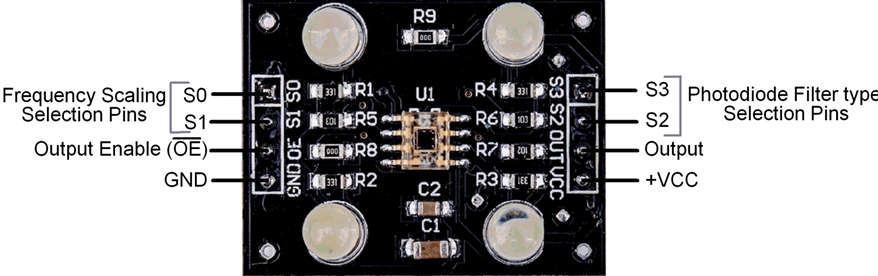
- Color Sensor Module has 4 LEDs with TCS3200 Color Sensor IC.
- The module is designed in such a way that 4 bright LEDs will light the object and reflections from that object will strike the TCS3200 Color Sensor IC to detect the color of an object.
- TCS3200 is a programmable color-to-frequency converter, that gives square wave output with frequency directly proportional to the light sensitivity.
- It consists of an 8×8 array of photodiodes i.e. 64 photodiodes.
- Of the total 64 photodiodes, 16 photodiodes have Red filters, 16 photodiodes have Green filters, 16 photodiodes have Blue filters, and 16 photodiodes are Clear with No filters.
- All photodiodes of the same color are connected in parallel.
- This sensor gives us object color in form of RGB (Red, Green, Blue) values, from which we can define the object color.
Block Diagram and Pin Diagram

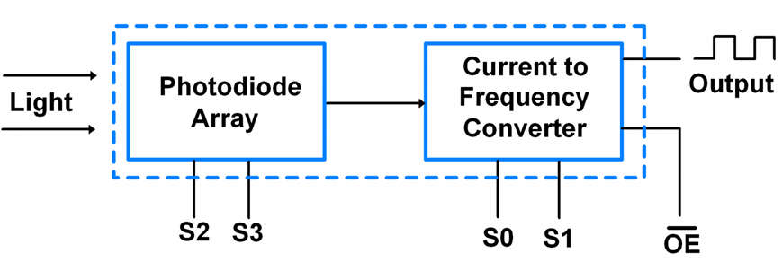
Pin 1:2 – S0:S1: Output frequency scaling selection pins.
- These two pins are used to scale the frequency of the current to the frequency converter.
Pin 3 – OE (Active Low): Output Enable
- 0= Output pin is enabled.
- 1= Output pin is in High-Impedance state.
Pin 4:5 – GND: VCC

- GND= Power Supply Ground.
- VCC= Supply Voltage to the sensor.
Pin 6 – Output
- This pin gives output in the form of a train of pulses. The duty cycle of these pulses is fixed to 50% and the frequency of these pulses is varying according to the input light.
Pin 7:8 – S2:S3 – Photodiode filter type selection pins

Applications of TCS 3200
- TCS3200 is applied for industrial process control.
- In laser edge banding machines to detect color TCS3200 is used.
- To detect chronic kidney diseases TCS3200 is used for urine analysis.
- TCS3200 is used in fruit sorting systems.
- The intensity of blue, red, and green radiations can be measured using this sensor module.