

- The CD4071 is a four-OR gate CMOS chip. Each OR gate has two inputs, and the chip contains four gates. It’s also known as a Quad 2-Input OR Gate.

- First of all, we will understand what is OR gate and what is its function.
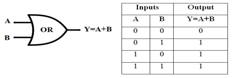
- The OR gate is a common type of digital logic circuit. When both input states are low, the OR gate’s output state is always low. Simply put, if any input value in the OR gate is set to 1, the output will always be high-level (1).
- The logic or Boolean expression for the OR gate is the logical addition of inputs, denoted by the plus sign (+), as shown below.
A+B=Y - The value of Y will be true when one of the inputs is set to true.

- Now coming back to the CD4071 IC, it has 14 pins and is available in Dual-in-line ceramic packages.


ADVERTISEMENT
- CD4071 quad gates are monolithic complementary MOS (CMOS) integrated circuits made up of N- and P-channel enhancement mode transistors. They have equal source and sink current capabilities and adhere to B series output drive standards.
- Additionally, the devices have buffered outputs, which improve transfer characteristics by providing extremely high gain. All inputs are protected against static discharge by diodes connected to VDD and VSS.
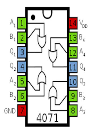
Pin Configuration
- The pin diagram of CD4071 OR gate IC is shown below.

| PINS | FUNCTIONS |
|---|---|
| A1 | Pin 1 will be used as the first input pin for the first OR gate in IC CD4071. |
| B1 | Pin 2 will be used for the second input pin for the first OR gate in IC CD4071. |
| Q1 | The output of the first OR gate will be received at Pin 3. |
| Q2 | Pin 4 will be used to receive the output of the second OR gate from IC CD4071. |
| A2 | Pin 5 will be used for the first input pin of the second OR gate in IC CD4071.. |
| B2 | Pin 6 will be used to give the second input to the second OR gate in IC CD4071. |
| GND | Pin 7 is a ground pin; it will be used as common ground by other communication devices with IC and Power Supply. |
| A3 | Pin 8 will be used to give the first input to the third OR gate to the IC. |
| B3 | Pin 9 will be used to give the second input to the third OR gate to the IC. |
| Q3 | Pin 10 will be used to receive the output of the third OR gate from the IC. |
| Q4 | Pin 11 will be used to receive the output of the fourth OR gate from the IC. |
| A4 | Pin 12 will be used as the first input pin of the fourth OR gate. |
| B4 | Pin 13 will be used as the second input pin of the fourth OR gate. |
| VDD | The Power Supply will be provided at pin 14 to make the IC functional. |
Features of CD4071 OR Gate IC
- Low power TTL compatibility: Fan out of two 74L or one 74LS.
- parametric rating 5V-10V-15V.
- Characteristics of symmetrical output.
- Maximum input leakage of 1 A at 15V over the entire temperature range.
Application of CD4071 OR Gate IC
- C4071 is used in digital electronics to build logic-level circuits.
- When you need OR operation in a low-power application with a wide voltage range, this IC is a good choice.
- It is also used in the creation of encoders and decoders.
- This IC can also be used in applications that require the checking of multiple events.
- It can also be used in applications where the temperature is to be observed as CD4071 can detect temperature and variables.
