

Introduction
A quad bilateral switch IC is an electronic component that contains four independent analog switches. These switches allow signals to pass in both directions when enabled, making them highly useful in analog signal processing applications.
Pin Configuration
| Pin Number | Pin Name | Description |
|---|---|---|
| 1, 4, 8, 11 | IN/OUT SIG A, B, C, D | Input/Output pins for switches A, B, C, and D |
| 2, 3, 9, 10 | OUT/IN SIG A, B, C, D | Output/Input pins for switches A, B, C, and D |
| 7 | Vss | Ground of the circuit |
| 14 | Vdd | Power supply voltage |
| 5 | CONTROL_B | Control input for Switch B |
| 6 | CONTROL_C | Control input for Switch C |
| 12 | CONTROL_D | Control input for Switch D |
| 13 | CONTROL_A | Control input for Switch A |
Working Principle
The quad bilateral switch IC operates based on control signals applied to its control pins. Each switch (A, B, C, and D) can be independently turned ON or OFF using its respective control input.
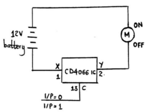


- When a control input is HIGH, the corresponding switch is turned ON, allowing signals to pass between the input and output pins.
- When a control input is LOW, the switch is turned OFF, blocking the signal path.
Since the switches are bilateral, signals can flow in either direction through the switch when it is ON.
Key Features
- Four independent analog switches in a single IC
- Bidirectional signal flow capability
- Controlled using digital logic signals
- Low power consumption
- Suitable for analog and digital applications
Applications
- Signal routing and multiplexing
- Analog switching circuits
- Sample and hold circuits
- Audio signal switching
- Data acquisition systems
Conclusion
The quad bilateral switch IC is a versatile component widely used in electronic circuits for switching and signal control. Its ability to handle bidirectional signals and operate with simple control inputs makes it ideal for various communication and signal processing applications.