


Dynamic Random Access Memory (DRAM) implements a series of capacitors that are meant to store individual bits for Random Access Memory (RAM). RAM is a type of memory that can access a data element regardless of its position in a sequence. So, in essence, the time it takes to access any data is constant. An optimal design of access transistors and storage, capacitors as well as advancement in semiconductor processes have made DRAM storage the cheapest memory available. As stated earlier DRAM is most often employed as a computer’s main memory due to its cost-effectiveness as compared to SRAM counterparts. DRAM technology has gone through some major revisions over the decades to drastically reduce cost-per-bit, increase clock rate, and reduce the overall dimensions of this component. These improvements can be associated with a number of changes including the introduction of the smaller DRAM cell, synchronous DRAM architectures, and finally DDR topologies.
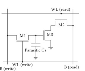
A typical 3-transistor DRAM cell employs the use of access transistors and a storage transistor to switch the input capacitance of the storage transistor on (bit value 1) and off (bit value 0). The array of transistors are tied to read and write columnlines and rowlines that are also known as bitlines and wordlines respectively. The components and data lines are arranged in such a way that allows for both write and read operations with a singular storage transistor.

For instance, a traditional 3-transistor DRAM cell (Figure 1) performs a write command by sending voltage to the gate of the M1 access transistor which, in turn, charges the gate capacitance of M3. The write line is then driven low and the charge stored in the gate capacitance of M3 slowly dissipates–thus the term dynamic.


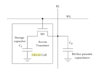
Current technologies will often employ a 1-transistor/1-capacitor (1T1C) memory cell (Figure 1) for more densely packed memory chips. The CMOS gate is tied to the word line while the source is tied to the bit line. A write command is accomplished by turning the gate to the transistor on thereby sending current to the discrete storage capacitor. A read is accomplished by sharing the charge stored in the capacitor with the bit line. The architecture requires a rewrite (refresh) after every read operation as the charge sharing destroys the information contained in the DRAM cell. Typically, this recharge happens every few milliseconds to compensate for charge leaks from the capacitor.
Asynchronous Switching Waveforms
The real complexity of this technology lies several layers of hierarchy up where an array of thousands of cells need to be tracked and assessed for various operations such as writes, reads, and refreshes. Current DRAM technology utilizes multiplexed addressing where the same address input pins are leveraged for both the row and column addresses, this ultimately saves space and lessens pin count.
The operations performed through the use of a Row Address Strobe (RAS) and a Column Access Strobe (CAS) clock. The RAS validates that the signal sent to the DRAM is, in fact, a row address while the CAS validates input column addresses. On the falling edge of the RAS, the address present on the DRAM address pins are inputted into the row address latches. On the falling edge of the CAS, the addresses are inputted into the column address latches on its falling edge. In essence, turning on an entire row (in the memory array) allows the information stored on the capacitors to be read (sensed), or, allows the charging/discharging of the storage capacitors for a write.
This is accomplished to through the use of a number of peripheral circuits including row/column latches, row address buffers, row/column decoders, wordline drivers, and bitline sense amplifiers. In the case of the 1T1C DRAM cells, a sense amplifier is often used as a row buffer to prevent the loss of information in the DRAM cells that are read (every read destroys the information in that DRAM cell). Sense amplifiers essentially senses whether or not the storage capacitor has adequate charge and then, takes a low power signal and amplifies it to a full logic value (0 or 1). A selected row in memory cannot be accessed until the informations is loaded and stored into the sense amplifiers. This is what leads to CAS latency where if the desired row is not active by the time it is requested, additional time is required.
As shown in Figure 2, in the first step, when the RAS is low, all the cells in an entire row is read by its sense amplifier–a process that takes a relatively long time. After this, the row is active so that the columns may be accessed for a read or write. Access time (read/write cycle time) for the is RAS is generally much higher than a CAS due to the sense amplifying step. Bus speeds for asynchronous DRAMs typically do no exceed 66 MHz.
SDRAM vs DRAM
DRAM operate in either a synchronous or an asynchronous mode. In the synchronous mode all operations (read, write, refresh) are controlled by a system clock. This system clock is synchronous with the clock speed of the CPU of a computer (~133 MHz). The reason for this is that it actually allows for much higher clock speeds (3x) than conventional DRAM. All operations to and from the DRAM are executed at the rising edge of a master clock. The typical single data rate (SDR) SDRAM clock rates are 100 and 133 MHz.
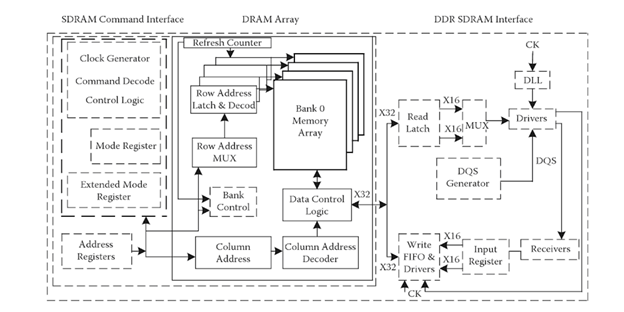
One major differentiating factor in SDRAM architectures is the memory being divided into a number of sections of equal size. These memory banks can perform access commands simultaneously, allowing for much greater speeds than the average DRAM. As shown in Figure 3, the basic core and operations of the DRAM is essentially the same, the synchronous interleave involved an I/O command interface coming separately from the DRAM chip.
The major contribution to the enhanced speeds of SDRAMs come from the concept of pipelining–while one bank may be in a precharging stating going through access latency, reading may be taking place in another bank so that the memory chip is constantly outputting data. In other words, the architecture of multiple banks allows for concurrent access of different rows.
DDR vs SDRAM
While the clock rate of a single data-rate (SDR) SDRAM–often referred to as simply SDRAM–would suffice for many applications, they are often not nearly enough for multimedia applications. The next iteration of the SDRAM was the double-data-rate SDRAM (DDR SDRAM). Where the primary evolution came with the ability to transfer data on both the rising and falling edges of the master clock while all commands and operations took place only on the rising edge of the clock–effectively sending twice the data per clock cycle.
This is accomplished through a prefetching operation where the wide internal bus prefetches two bits (words) of data simultaneously to burst two words of equal width out on the I/O pins. Also known as a 2-bit prefetch, this essentially doubles the data rate without increasing the power consumption of the memory unit. It should also be noted that there is a marked improvement in power efficiency with the DDR architectures, where DDR2 runs at 2.5V, DDR3 at 1.5V to 1.65V, and DDR4 at 1.2V. This is due to the revisions in the power management circuitry of the device as well as the ability to more smartly increase the frequency of data transfers without increasing power consumption. The reduction in power consumption allow DDR modules to be a more desirable option for computers that can run off of battery power (e.g.: a laptop).
DDR vs DDR2 vs DDR3 vs DDR4
The underlying components and functionality/operations for the later evolutions of DDR (DD2, DD3, DDR4) remains the same with the differentiating factor of an increase in clock speed. For instance, a DDR2 RAM added a 2x clock multiplier to the DDR SDRAM interface thereby doubling data transfer speeds while maintaining the same bus speed. This way a ‘4-bit prefetch’ is employed from the memory array to the I/O buffer. Along the same lines 8 bits of data are prefetched in DDR3 modules and 16 bits for DDR4 modules.

While the core of the volatile DRAM architecture has remained essentially the same, the additional command interfaces off-chip has evolved increased capacity and decreased cost-per-bit. This major evolutions in performance of DRAM could then be contributed to the pipelining of data as well as the increase in I/O buffer frequency.