

IC (Integrated Circuit) is one of the most important electronic components, due to the complex function and uses involved, there are many types Of ICs. To facilitate the management, IC chips were defined as various standard packages. IC packing indicates the dimension and shape of a chip. Chips with the same electronic parameters may have different package types. IC packages types are mainly divided into traditional DIP dual-in-line and SMD chip package.
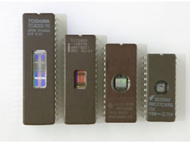
DIP (Double In-line package)
A Dual-in-line package (DIP or DIL), or dual-in-line pin package (DIPP) is an electronic component package rows of electrical connecting pins. The package may be through-hole mounted to a printed circuit board (PCB). The pin pitch of DIP is typically 15.2mm.


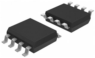
SOP/SOIC/SO (Small Outline Package)
A surface mounts integrated circuit package is known as SOIC. The standard form is a flat rectangular body, with leads extending from two sides. The leads are formed in a gull-wing shape to allow solid footing during assembly to a PCB.In Matte Tin plating standard Pb-free finish on these packages.From both sides of the body, the pins are drawn in an L shape. In addition to being used for memory LSI, SOP is also widely used in circuits. The pin pitch is 1.27mm. The number of pins is from 8 to 44.

Types of small outline package are
- Small Out-Line J-Leaded Package
- Thin Small Outline Package
- Shrink Small Outline Package
- Thin Shrink Small Outline Package
- Quarter-size Small Outline Package
- Very Small Outline Package
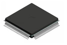
QFP (Quad Flat Package)
From four sides the leads are led out in an L-shape, plastic packaging accounts for the vast majority of the other materials are ceramic, metal. The pin pitches include 1.0mm, 0.8mm, 0.65mm, 0.5mm, 0.4mm and 0.3mm. The maximum number of pins of 0.65mm package is 304.

- Flat Quad Flat Package
- Thin Quad Flat Package
- Plastic Quad Flat Package
- Quad Flat Package with Bumper/Quad Flat Non-leaded Package
The four sides of this IC packaging are equipped with electrode contacts. The mounting area is smaller than QFP and the height is lower than QFPdue to the absence of leads
The number of electrode contacts is general from 14 to 100. The materials used are ceramic and plastic. When there is an LCC mark, it is a ceramic QFN, of which the spacing of electrode contacts is 1.27mm. Plastic QFN has different pin pitches of 0.65mm, 0.5mm, and 1.27mm, this package is also known as PLCC.
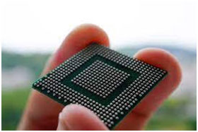
BGA (Ball Grid Array Package)
BGA IC is one of the most used and famous IC nowadays. Whenever the work is compact or where the minimization of the gadget is done this IC is used. Spherical bumps are formed on the back surface of the printed substrate to replace the lead. The LSI chip is mounted on the front surface of the PCB board, and then sealed by a molding resin or a potting method; the numbers of pins can exceed 200.

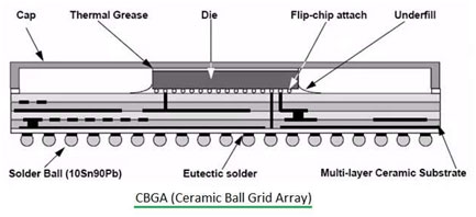
1.CBGA (Ceramic BGA)
- As the name implies, this is made up of Ceramic chips. The life of this type is not long. The ratio between tin and lead is 10:90 in this type. Because of a very high melting point, this type of BGA requires a C4 Approach for making the bridge between BGAs and PCBs. The cost is a little high than that of PBGAs but this type of BGA is extremely reliable for better electrical performance and better thermal conductivity. This type was very much famous in past.
2.FBGA (Fine BGA)
- Fine Ball Grid Array based on ball grid array technology. It is widely used nowadays in mobiles, computers, and laptops. It is also known as a system-on-chip IC. It has thinner contacts; it is also known as Fine Pitch Ball Grid Array.
3,LBGA (Low-profile BGA)
- Low-profile BGA has a short life span. It’s like CBGA but is the design on normal PCB and its updated version is LFBGA (Low-profile Fine-pitch BGA)
4.FC-BGA (Flip Chip Ball Grid Array)
- Flip chips useful for high-frequency applications because the chip rests right on the circuit board and is quite small, so there is less inductance and signal speeds can be higher. They also have better moisture resistance and thermal conductivity. This process is often considered a desirable alternative to standard wire bonding BGA packages. Flip-chip components are used most commonly in semiconductor operations.
4.PBGA (Plastic BGA)
- PBGA stands for Plastic Ball Grid Array. These are being used recently which are the most popular type for double-sided PCBs. MOTOROLA invented the first PBGA and now it is widely used by almost all manufacturers.it can carry from 200 to 500 ball arrays. This BGA had good capacity. This BGA follows level 3 criteria. This along with the application of OMPAC and GTPAC is highly reliable and is verified by JEDEC.
5.EBGA (Enhanced Ball Grid Array)
- EBGA is the summation of PBGA and additional heat sink options. Chips are always faced down and wire bond is used for conduction between PCB & chips are used in these types of BGA.
6.TBGA (Tape BGA)
- TBGA is used in making thin products that have strong core materials with better heat dissipation and superlative electrical connectivity properties. The only advantages PBGA has over TBGA are that TBGA always costs higher than PBGA. PCBs used in this type of BGA are girded plastic.
7.MBGA (Metal BGA)
- In these types, the substrate which is used is metal-ceramic. Circuits are made up of sputtering coating and chips are faced down. Wire bonding is used to make the connection. This array is very good for better electrical performance as well as thermal heat dissipation values.
8.Micro BGA
- In this approach, chips are always faced down while the substrates are made up of packaging tape. Tessera Company has invented Micro BGA. They are named mini-sized and that is the most important value of Micro BGA. It allows the manufacturers to plans for high-tech yet small-sized products. On top of that, this type is the core of higher storage products while the numbers of pins are low. Therefore, better accessibility while lower liability.
CSP (Chip Scale Package)
CSP is the most famous IC and it is way better and improves than BGA. This IC is very small in size. Compared to the BGA, the storage capacity of the CSP package in the same space can increase by three times.
This IC packaging can reach a close to 1:1 ratio of chip area to package. The absolute size is only 32 square millimeters, which is about 1/3 of the ordinary BGA, 1/6 of the chip area to TSOP memory CSP is just an IC packaging standard, every package type that reaches this ratio can be called CSP. Whether a PCB assembly house can deal with the CSP IC packaging or not reflects its assembly capabilities.

Types of Chip scale packages
- Customized lead frame-based CSP
- Flexible substrate-based CSP
- Flip-chip CSP
- Rigid substrate-based CSP
- Wafer-level redistribution CSP