

A PN-junction diode is formed when a p-type semiconductor is combined with an n-type semiconductor creating a potential barrier voltage across the diode junction. P-type semiconductor and N-type semiconductor acts as a resistor but by doing one side of silicon crystal with a p-type impurity and the other side by the n-type impurity, we can convert the silicon crystal into PN junction. And that junction has a border where the p-type and n-type region meets. This silicon crystal with p-type and n-type impurity is also known as the diode. Because the p-type and n-type region acts like two electrodes.
A PN Junction Diode is one of the simplest semiconductor devices all around, and it has the characteristic of passing current in only one direction. Though, unlike a resistor, a diode does not act linearly concerning the applied voltage as the diode has an exponential current-voltage ( I-V ) relationship.
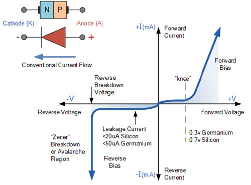
Junction Diode Symbol and Static I-V Characteristics
There are two operating regions and three possible “biasing” conditions for the standard Junction Diode and these are
Zero Bias
At zero bias no external voltage potential is applied to the PN junction diode.
Reverse Bias
At reverse bias the voltage potential is connected negative, (-ve) to the P-type semiconductor material and positive, (+ve) to the N-type semiconductor material across the diode which has the effect of Increasing the width of the PN junction diode.
Forward Bias
At forwarding bias the voltage potential is connected positively, (+ve) to the P-type semiconductor material and negative, (-ve) to the N-type semiconductor material across the diode which has the effect of Decreasing the width of PN junction diodes.
V-I characteristics
The graph between the voltage applied across the diode terminals and the current that flows through it is called V-I characteristics of the diode. This graph is divided into parts.
- Forward characteristics
- Reverse characteristics
Forward characteristics
In forward characteristics of the diode, the positive terminal of the voltage source is connected with P-side and the negative terminal of the voltage source is connected with the N-side of the diode. After applied the forward bias condition, if we gradually increase the voltage across the diode in small steps of 0.1 V and record the corresponding value of diode current. And after finding the voltage and current values plot the graph such that voltage across the diode along the horizontal axis and diode current along the vertical axis then we get the curve. The curve obtains so far is known as the forward characteristics of the P-N junction diode.
We know that in the forward bias condition when we increase the forward voltage the depletion layer reduces. The voltage at which the depletion layer width becomes zero that stage is called as knee voltage of the diode. It can also be defined as the voltage at which the diode starts conducting is called knee voltage and before this knee voltage, the current through the circuit is almost zero. This knee voltage is also known as threshold voltage or cut-in voltage. After this knee voltage, the current through the diode increases exponentially. Knee voltage is 0.3V for a germanium diode and 0.7V for a silicon diode.
Reverse characteristics
In reverse characteristics of the diode, the positive terminal of the voltage source is connected with N-side and the negative terminal of the voltage source is connected with the P-side of the diode. In reverse bias, the applied voltage is gradually increased in suitable steps and the value of current is recorded in each step. After recording we plot a graph with reverse voltage along the horizontal axis and diode current along the vertical axis. The obtained curve indicates that initially the current increases with applied reverse voltage to a small value. This small value of current is called Reverse Saturation Current, it is denoted by I0. It is nano amperes for Si diode and microamperes for Ge diode. If we increase the reverse voltage the current remains constant till a voltage is reached called breakdown voltage and it is represented by VBR. After the breakdown voltage, the reverse current increases abruptly. These are called reverse characteristics of the P-N junction diode.
Advantages of PN junction diode
- It is smaller in size.
- It can be operated at low voltage.
- It is strong and cannot be destroyed easily.
- It requires no time to warm up to produce the current carriers since it is a semiconductor.
- It is cheap.
Disadvantages of PN junction diode
- It is a non-ohmic conductor.
- When it is polarized, only a very small current flows.