- The CD4066 device is a quad bilateral switch intended for the transmission or multiplexing of an analog or digital signal.
- It exhibits a much lower on-state resistance, which is relatively constant over the full signal-input range.
- The CD4066 consists of four bilateral switches, each with independent controls.
- Both the p and the n devices in a given switch are biased on or off simultaneously by the control signal.
- The well of the n-channel device on each switch is tied to either the input (when the switch is on) or to VSS (when the switch is off).
- This configuration eliminates the variation of the switch-transistor threshold voltage with the input signal and, thus, keeps the on-state resistance low over the full operating-signal range.
Pin Diagram
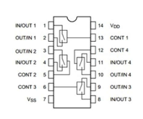
| PIN Number | PIN Name | Description |
|---|---|---|
| 1, 4, 8, 11 | IN/OUT SIG A, B, C, | Input/ Output pin for Switch A, B, C and D |
| 2, 3, 9, 10 | OUT/IN SIG A, B, C, D | Output/ Input pin for Switch A, B, C and D |
| 7 | Vss | Ground of the circuit. |
| 14 | Vdd | Voltage Supply |
| 5 | CONTROL_B | switch-B Control input |
| 6 | CONTROL_C | switch-C Control input |
| Pin 12 | CONTROL_D | switch-D Control input |
| Pin 13 | CONTROL_A | switch-A Control input |
Working of CD4066 Quad Bilateral Switch IC
- The CD4066 IC consists of four switches. It can switch analog signals through digital control.
An analog signal is applied at the input of the switch. - If a HIGH or 1 value is fed into the control input, the analog signal will be passed from the input to the output of a switch.
- As it is a bilateral switch, therefore it can operate in both directions forward and reverse.
- Each switch has two pins which can be used as both input and output for switching voltages.
- Pin 14 is connected to the positive terminal of the voltage supply.
- pin 7 is connected to the ground of the circuit.
- When the control input
- HIGH or 1, the terminals of the switch have low impedance between them, and they are said to be in ON condition.
- LOW or 0, the switch is OFF, and the terminal is connected by High impedance.
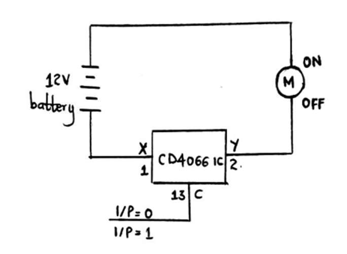
- The motor remains in an off state when there is no control signal.
- As we apply a logic high control signal to a control pin of switch A, the motor starts to move.
- Therefore, the basic purpose of using this ic is to isolate the control signal from the power signal.
- This IC can also be used as a 4×1 multiplexer.
Applications of CD4066 Quad Bilateral Switch IC
- You can use it as 4 input multiplexer IC.
- Switching and multiplexing of Analog Signals and Digital Signals.
- Sample and Hold circuits.
- Switching of networks.
- Signal Gating, Modulators, Demodulators, Choppers, Commutating Switches.
- Logic Implementation of Transmission-Gates.