• Home
  • About Us
  • Contact Us
Semiconductor for You
  • Home
  • Semiconductor News
  • Technology
    • Automotive
    • Consumer Electronics
    • IoT
    • Lighting
    • Power Management
    • Wireless
    • Personal Electronics
    • Hardware & Software
    • Research
    • Medical Electronics
    • Embedded Design
    • Aerospace & Defence
    • Artificial Intelligence
  • DIY Projects
  • Market
  • Industries
    • Renesas Electronics
  • Knowledge Base
  • Events
  • Tools
    • Resistor Color Code Calculator
No Result
View All Result
Semiconductor for You
No Result
View All Result
Home Articles

How PN junction is formed?

Semiconductor For You by Semiconductor For You
May 25, 2021
in Articles
0
ADVERTISEMENT

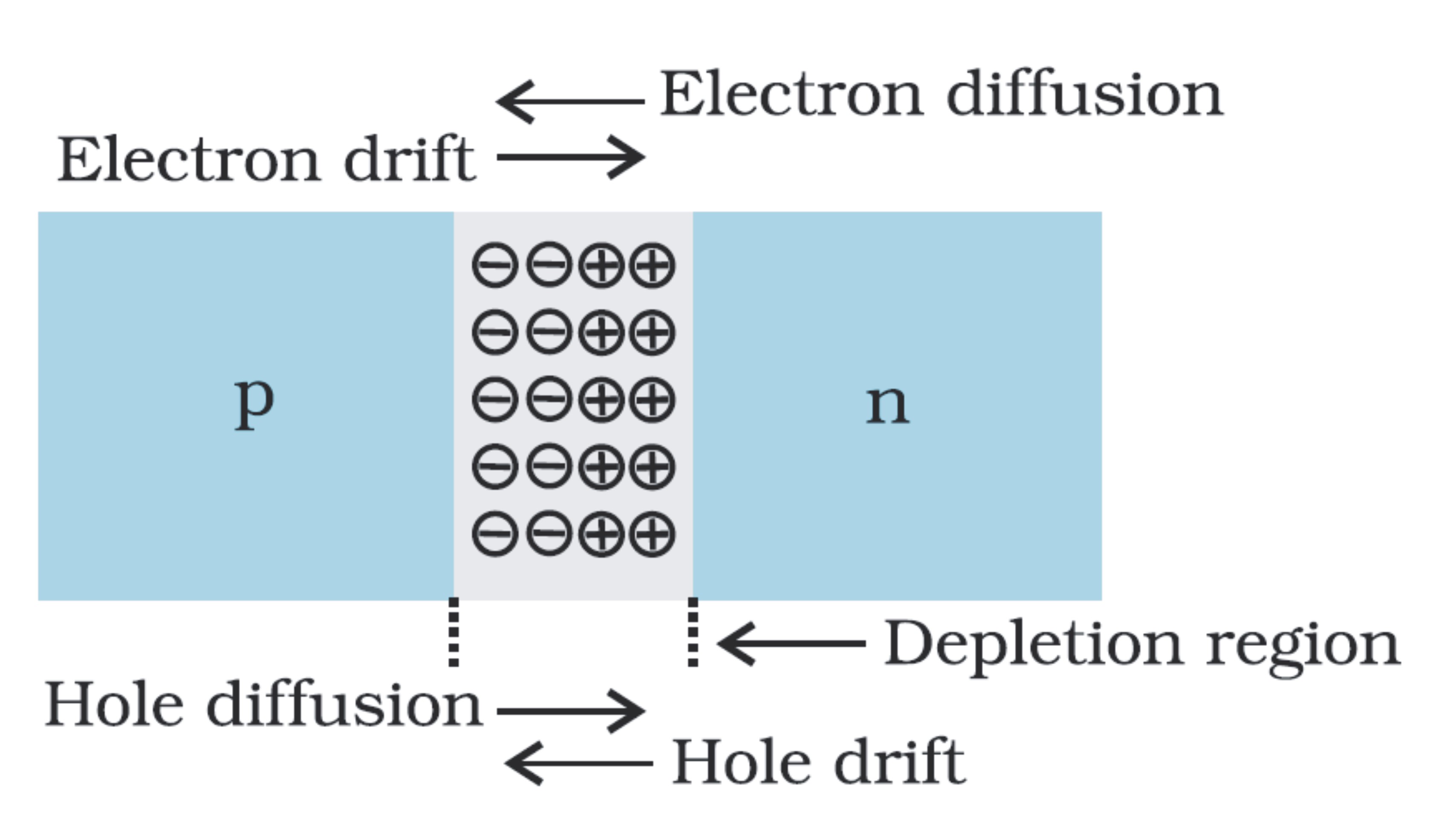
A P-type and N-type semiconductor are joint together with a help of special fabrication techniques to form a PN-Junction. The terminals are brought out for external connection with P-type and N-type semiconductor. The P side is called as anode and N side is called as cathode. The PN Junction forms a basic semiconductor device called diode. In a PN-junction, when the electrons and holes move to the other side of the junction, they leave behind exposed charges on dopant atom sites, which are fixed in the crystal lattice and are unable to move. The electric field Ê forms between the positive ions cores in the n-type material and negative ion cores in the p-type material. This electric field created by the diffusion process has created a “built-in potential difference” across the junction with an open-circuit (zero bias) potential of:

Where

Eo is the zero bias junction voltage.

VT is the thermal voltage of 26mV at room temperature.

ND and NA are the impurity concentrations.

ni is the intrinsic concentration.


Content Protection by DMCA.com
Tags: PN junctionSemiconductors
Semiconductor For You

Semiconductor For You

Browse by Category

  • Aerospace and Defence
  • Articles
  • Automotive
  • Consumer-Electronics
  • Hardware & Software
  • Interview
  • IoT
  • Knowledge Base
  • Lighting
  • Market
  • personal-electronics
  • Power Management
  • Research
  • Semiconductor Events
  • Semiconductor News
  • Technology
  • Wireless
Semiconductor for You

Semiconductor For You is a resource hub for electronics engineers and industrialist. With its blend of
technology features, news and new product information, Semiconductor For You keeps designers and
managers up to date with the fastest moving industry in the world.

Follow Us

Browse by Category

  • Aerospace and Defence
  • Articles
  • Automotive
  • Consumer-Electronics
  • Hardware & Software
  • Interview
  • IoT
  • Knowledge Base
  • Lighting
  • Market
  • personal-electronics
  • Power Management
  • Research
  • Semiconductor Events
  • Semiconductor News
  • Technology
  • Wireless

Recent News

Infineon Strengthens NewSpace Capabilities with Launch of LEO-Optimized Memory Products

Infineon Strengthens NewSpace Capabilities with Launch of LEO-Optimized Memory Products

June 18, 2025
Fujitsu awarded contract to design next-generation flagship supercomputer FugakuNEXT

Fujitsu awarded contract to design next-generation flagship supercomputer FugakuNEXT

June 18, 2025
  • About
  • Advertise
  • Privacy & Policy
  • Contact

© 2022 Semiconductor For You

No Result
View All Result
  • Home
  • Semiconductor News
  • Technology
    • IoT
    • Wireless
    • Power Management
    • Automotive
    • Hardware & Software
  • Market
  • Knowledge Base
  • Tools
    • Resistor Color Code Calculator

© 2022 Semiconductor For You