Introduction
An Active Pixel Sensor (APS) is an image sensor that consists of an array of pixel sensors, where each pixel contains a photodetector and an amplifier. One of the most widely used types of APS is the CMOS Active Pixel Sensor (CMOS APS).
CMOS APS is commonly used in modern imaging devices such as digital cameras, webcams, and DSLR cameras. It is called CMOS APS because it is manufactured using Complementary Metal-Oxide-Semiconductor (CMOS) technology. This type of sensor is similar to Charge Coupled Devices (CCD) but offers several advantages in terms of power consumption and integration.

Working Principle of CMOS APS
CMOS Active Pixel Sensors work by detecting light using a photodetector within each pixel. When light falls on the sensor, it is converted into an electrical signal. This signal is then amplified using transistors present within the pixel and transmitted through standard electrical connections. Each pixel operates independently, allowing faster processing and reduced noise compared to earlier technologies.
Development of CMOS APS
The widespread use of CMOS Active Pixel Sensors began around 1993, when prototypes developed by the Jet Propulsion Laboratory were commercialized. Due to their advantages in high-speed and low-power imaging, many companies quickly adopted this technology.
Before the development of active pixel sensors, passive pixel sensors were used. These lacked individual amplifiers in each pixel, leading to higher noise, slower performance, and greater power consumption. The introduction of APS significantly improved image quality and efficiency. With the advancement of CMOS technology in the 1990s, CMOS APS became the foundation for modern imaging systems and digital electronics.
Architecture of CMOS Active Pixel Sensor
The architecture of CMOS APS can be understood through three main components:
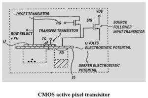
1. Pixel Structure
Each CMOS APS pixel typically consists of a photodetector and multiple transistors. The most common configuration is the 4T (four-transistor) pixel, which includes:
- Transfer gate
- Reset gate
- Selection gate
- Source follower transistor
This design enables efficient charge transfer, low noise, and improved image quality. A simpler 3T (three-transistor) design is also used in some applications due to its lower manufacturing cost.
2. Thin Film Transistor (TFT) APS
Thin Film Transistor (TFT) technology is used in certain applications such as digital X-ray imaging. However, TFT-based sensors are limited due to their larger size and lower gain compared to CMOS APS.
3. Pixel Array
CMOS APS consists of a two-dimensional array of pixels arranged in rows and columns. The reset and selection lines are connected row-wise, while the output is read column-wise. This structure allows efficient scanning and processing of image data.
Advantages of CMOS APS
- Low power consumption
- High-speed image processing
- Integration with digital circuits on the same chip
- Reduced noise compared to passive sensors
- Cost-effective manufacturing
Limitations of CMOS APS
- Slightly lower image quality compared to CCD in some cases
- Complex pixel design
- Fixed pattern noise in early designs
Applications of CMOS APS
- Web cameras
- Motion capture cameras
- Digital radiography
- Endoscopic cameras
- X-ray imaging systems
- Digital and filmless cameras
Conclusion
CMOS Active Pixel Sensor technology has revolutionized modern imaging systems by providing high-speed, low-power, and cost-effective solutions. With continuous advancements, CMOS APS has become the preferred choice for a wide range of applications, from consumer electronics to medical imaging.