• Home
  • About Us
  • Contact Us
Semiconductor for You
"
  • Home
  • Semiconductor News
  • Technology
    • Automotive
    • Consumer Electronics
    • IoT
    • Lighting
    • Power Management
    • Wireless
    • Personal Electronics
    • Hardware & Software
    • Research
    • Medical Electronics
    • Embedded Design
    • Aerospace & Defence
    • Artificial Intelligence
  • DIY Projects
  • Market
  • Industries
    • Renesas Electronics
  • Knowledge Base
  • Events
  • Tools
    • Resistor Color Code Calculator
No Result
View All Result
Semiconductor for You
No Result
View All Result
Home Semiconductor News

Critical EUV Milestone: Implications For Semiconductors

Semiconductor For You by Semiconductor For You
July 17, 2017
in Semiconductor News
0
ADVERTISEMENT

ASML successfully demonstrated a 250-watt EUV source recently.

The company is claiming affordable use relative to conventional technologies.

Industry observes are divided on EUV’s realizable cost benefits.

EUV,if cost effective, will change the dynamics of semicondutor supply line.

ASML Holding (ASML) recently achieved a key milestone by demonstrating a 250-watt extreme ultraviolet lithography, or EUV, source at Semicon West Trade show. It’s quite a big deal as hitting the 250-watt mark was the key barrier in driving a material throughput using EUV process. However, it should be noted that productivity of EUV system also depends on “availability” that relates to debris management.
Picture Credit: eetimes

Michael Lercel, director of strategic marketing at ASML, said the company has demonstrated 250 watts “rather consistently by really understanding the conversion efficiency in the source and putting the right controls in place.” The source is not being shipped as of now.

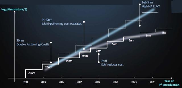
EUV has been in the spotlight for years as the technology can eliminate the need for multi-patterning in semiconductor manufacturing that can result in lower manufacturing costs.

Note that shrinking the node has been putting quite a pressure on semiconductor manufacturer’s spending budget in recent times. The cost to design a 7nm chip is nine times higher than designing a 28nm chip; multi-patterning is the key contributor for such cost disparity.

Although EUV tools are expensive – around $100 million each – a 250-watt source will turn the cost benefit in EUV’s favor compared to multi-patterning using immersion lithography tools. With a 250W source, an EUV stepper can be able to process ~100 wafer-per-hour, which should allow for affordable use when matched with other lithography technologies.

Content Protection by DMCA.com
Semiconductor For You

Semiconductor For You

Browse by Category

  • Aerospace and Defence
  • Articles
  • Automotive
  • Consumer-Electronics
  • Hardware & Software
  • Interview
  • IoT
  • Knowledge Base
  • Lighting
  • Market
  • personal-electronics
  • Power Management
  • Research
  • Semiconductor Events
  • Semiconductor News
  • Technology
  • Wireless
Semiconductor for You

Semiconductor For You is a resource hub for electronics engineers and industrialist. With its blend of
technology features, news and new product information, Semiconductor For You keeps designers and
managers up to date with the fastest moving industry in the world.

Follow Us

Browse by Category

  • Aerospace and Defence
  • Articles
  • Automotive
  • Consumer-Electronics
  • Hardware & Software
  • Interview
  • IoT
  • Knowledge Base
  • Lighting
  • Market
  • personal-electronics
  • Power Management
  • Research
  • Semiconductor Events
  • Semiconductor News
  • Technology
  • Wireless

Recent News

Infineon SEMPER™ NOR Flash memory family achieves ASIL-D functional safety certification

Infineon SEMPER™ NOR Flash memory family achieves ASIL-D functional safety certification

May 9, 2025
onsemi’s AR0145CS Hyperlux SG Image Sensors, Now at Mouser

onsemi’s AR0145CS Hyperlux SG Image Sensors, Now at Mouser

May 8, 2025
  • About
  • Advertise
  • Privacy & Policy
  • Contact

© 2022 Semiconductor For You

No Result
View All Result
  • Home
  • Semiconductor News
  • Technology
    • IoT
    • Wireless
    • Power Management
    • Automotive
    • Hardware & Software
  • Market
  • Knowledge Base
  • Tools
    • Resistor Color Code Calculator

© 2022 Semiconductor For You