
Breakthrough Gen3 UCIe IP subsystem achieves 64 Gbps per-I/O pin data rates and doubles shoreline bandwidth density, enabling scalable XPUs, and data center chiplet architectures with TSMC’s 3nm process.
LONDON, United Kingdom, and TORONTO, Canada – September 24, 2025 – Alphawave Semi (LSE: AWE), a global leader in high-speed connectivity and compute silicon for the world’s technology infrastructure, today announced the successful tapeout of the industry’s leading 64 Gbps UCIe™ die-to-die (D2D) IP subsystem on TSMC’s 3nm process technology. Building on its 36 Gbps Gen2 silicon success, this third-generation subsystem delivers a major advancement in performance and shoreline bandwidth density for the IP Ecosystem. With 64 Gbps per-lane uni-directional data rates, it enables the next generation of chiplet-based architectures for AI, XPUs, and data center systems, providing power-efficient, reliable multi-die SoC integration and seamless interoperability across the chiplet ecosystem.
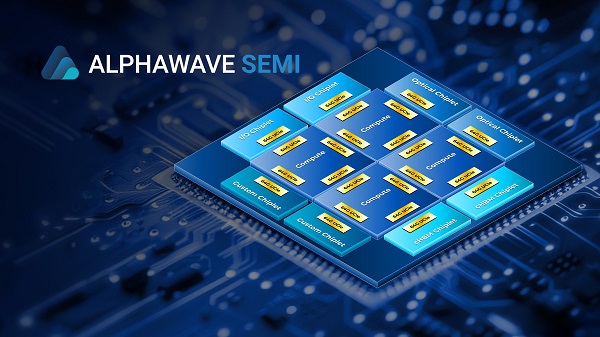
As the first 64 Gbps UCIe™ IP subsystem implemented on TSMC’s 3nm process, this achievement positions Alphawave Semi as a leader in UCIe die-to-die connectivity technology. With enhanced 64 Gbps UCIe performance and reduced power consumption, the solution enables new applications, including optical connectivity for Co-Packaged Optics (CPO), which are essential for scalable systems and environments requiring high lane count radix. Furthermore, it expands D2D interconnect capabilities, supporting a custom memory interface that delivers very low power and latency with a unique form factor, offering eight times greater bandwidth density compared to conventional memory interfaces.
Built on a silicon-proven architecture spanning multiple process nodes, Alphawave 64 Gbps UCIe delivers twice the bandwidth density of previous UCIe, achieving up to 3.6 Tbps/mm shoreline bandwidth in the Standard Package and more than 21Tbps/mm in the Advanced Package. This subsystem uses advanced architecture to enhance performance and reliability. With Alphawave’s proven D2D technology and adaptable firmware, customers can quickly develop and deploy chiplet-based solutions for changing market demands.
Alphawave offers an integrated D2D subsystem that supports protocols such as AXI-4, AXI-S, CXS, CHI, and CHI C2C, empowering flexible chiplet-based systems and providing a reference architecture for faster development. The 64 Gbps UCIe IP is fully compliant with UCIe 3.0 (released in August 2025). It includes robust test and debug features—iJTAG, BIST, DFT, Known Good Die (KGD), and live per-lane health monitoring—to ease customer integration and enhance reliability.
“The industry’s first tapeout of our Gen3 UCIe™ IP at 64 Gbps on TSMC’s N3P process marks a significant leap forward in die-to-die connectivity,” said Mohit Gupta, Executive Vice President & General Manager, Alphawave Semi. “Building on our success on the silicon for 36 Gbps UCIe IP at N3P, this achievement positions Alphawave Semi at the forefront of delivering ultra-high-performance and shoreline bandwidth density compared to prior generations. Just as importantly, it strengthens our broader AI platform—ensuring our suite of IP subsystems now delivers higher performance and efficiency than ever before on the 3nm process to meet the critical bandwidth demands of scalable AI compute.”
“Our collaboration with Alphawave Semi reflects our shared commitment to advancing high-performance, energy-efficient computing through leading design solutions on TSMC’s 3nm technology,” said Aveek Sarkar, Director of Ecosystem and Alliance Management Division at TSMC. “This achievement demonstrates how close collaboration with our Open Innovation Platform® (OIP) partners accelerates the delivery of advanced interface IP and custom silicon solutions to meet the rapidly growing demands of AI and cloud infrastructure.”
This tapeout marks a defining milestone for Alphawave Semi’s AI platform and chiplet reference architecture, establishing the foundation for the next generation of chiplet connectivity across hyperscaler, data center, and AI applications. The rapid progression from 36 Gbps to 64 Gbps on TSMC’s 3nm process reflects our leadership in advancing open, scalable chiplet ecosystems and our commitment to shaping the future of ultra-high-performance connectivity.
For further information on Alphawave Semi, please visit www.awavesemi.com.