• Home
  • About Us
  • Contact Us
Semiconductor for You
"
  • Home
  • Semiconductor News
  • Technology
    • Automotive
    • Consumer Electronics
    • IoT
    • Lighting
    • Power Management
    • Wireless
    • Personal Electronics
    • Hardware & Software
    • Research
    • Medical Electronics
    • Embedded Design
    • Aerospace & Defence
    • Artificial Intelligence
  • DIY Projects
  • Market
  • Industries
    • Renesas Electronics
  • Knowledge Base
  • Events
  • Tools
    • Resistor Color Code Calculator
No Result
View All Result
Semiconductor for You
No Result
View All Result
Home Semiconductor News

Application of air-sensitive semiconductors in nanoelectronics

Semiconductor For You by Semiconductor For You
September 28, 2017
in Semiconductor News
0
ADVERTISEMENT

A research group consisting of scientists from Tomsk Polytechnic University, Germany and Venezuela proved vulnerability of a two-dimensional semiconductor gallium selenide in air. This discovery will allow manufacturing superconducting nanoelectronics based on gallium selenide, which has never been previously achieved by any research team in the world.

The study was published in Semiconductor Science and Technology.
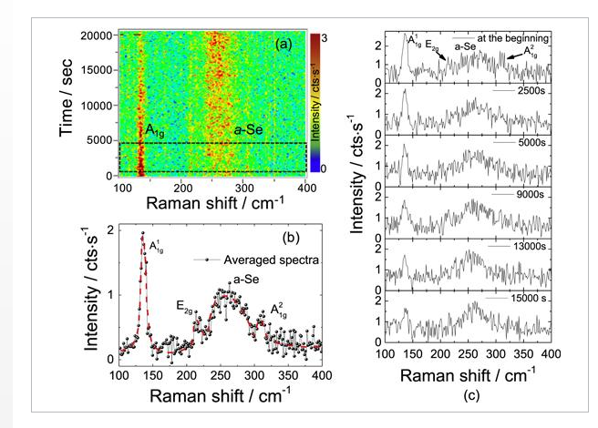
 

IMAGE: RAMAN SPECTRUM OF 8 L GASE TAKEN AT TWO DIFFERENT TIMES DURING TIME EVOLUTION MAP. (A) RED DASHED LINE IS DRAWN AS THE GUIDE FOR THE EYE. THE CONSTANT INTENSITY...
IMAGE: RAMAN SPECTRUM OF 8 L GASE TAKEN AT TWO DIFFERENT TIMES DURING TIME EVOLUTION MAP. (A) RED DASHED LINE IS DRAWN AS THE GUIDE FOR THE EYE. THE CONSTANT INTENSITY…


One of the promising areas of modern materials science is the study of two-dimensional (2D) materials, i.e. thin films consisting of one or several atomic layers. 2D materials due to their electrical superconductivity and strength could be a basis for modern nanoelectronics. Optic applications in nanoelectronics require advanced materials capable of ‘generating’ great electron fluxes upon light irradiation. Gallium selenide (GaSe) is one of the 2D semiconductors that can cope with this problem most efficiently.

‘Some research teams abroad tried to create electronic devices based on GaSe. However, despite extensive theoretical studies of this material, which were published in major scientific journals, the stability of the material in real devices remained unclear,’ says Prof. Raul Rodriguez, the Department of Lasers and Lighting Engineering.

The research team revealed the reasons behind this. They studied GaSe by means of Raman spectroscopy and x-ray photoelectron spectroscopy that allowed proving the existence of chemical bonds between gallium and oxygen. Photoluminescence in oxidized substance is absent that also proves the formation of oxides. It means that the scientists revealed that GaSe oxidizes quickly in air and loses its electrical conductivity necessary for creating nanoeletronic devices.

‘GaSe monolayers become oxidized almost immediately after being exposed to air. Further research of GASe stability in air will allow making proposals how to protect it and maintain its optoelectronic properties,’ emphasize the authors.

According to Prof. Rodriguez, for GaSe not to lose its unique properties it should be placed in a vacuum or inert environment. For example, it can be applied in encapsulated devices that are vacuum-manufactured and then covered with a protective layer eliminating air penetration.

This method can be used to produce next generation optoelectronics, detectors, light sources and solar batteries. Such devices of ultra-small sizes will have very high quantum efficiency, i.e. they will be able to generate large electron fluxes under small external exposure.

Content Protection by DMCA.com
Semiconductor For You

Semiconductor For You

Browse by Category

  • Aerospace and Defence
  • Articles
  • Automotive
  • Consumer-Electronics
  • Hardware & Software
  • Interview
  • IoT
  • Knowledge Base
  • Lighting
  • Market
  • personal-electronics
  • Power Management
  • Research
  • Semiconductor Events
  • Semiconductor News
  • Technology
  • Wireless
Semiconductor for You

Semiconductor For You is a resource hub for electronics engineers and industrialist. With its blend of
technology features, news and new product information, Semiconductor For You keeps designers and
managers up to date with the fastest moving industry in the world.

Follow Us

Browse by Category

  • Aerospace and Defence
  • Articles
  • Automotive
  • Consumer-Electronics
  • Hardware & Software
  • Interview
  • IoT
  • Knowledge Base
  • Lighting
  • Market
  • personal-electronics
  • Power Management
  • Research
  • Semiconductor Events
  • Semiconductor News
  • Technology
  • Wireless

Recent News

Infineon SEMPER™ NOR Flash memory family achieves ASIL-D functional safety certification

Infineon SEMPER™ NOR Flash memory family achieves ASIL-D functional safety certification

May 9, 2025
onsemi’s AR0145CS Hyperlux SG Image Sensors, Now at Mouser

onsemi’s AR0145CS Hyperlux SG Image Sensors, Now at Mouser

May 8, 2025
  • About
  • Advertise
  • Privacy & Policy
  • Contact

© 2022 Semiconductor For You

No Result
View All Result
  • Home
  • Semiconductor News
  • Technology
    • IoT
    • Wireless
    • Power Management
    • Automotive
    • Hardware & Software
  • Market
  • Knowledge Base
  • Tools
    • Resistor Color Code Calculator

© 2022 Semiconductor For You