• Home
  • About Us
  • Contact Us
Semiconductor for You
  • Home
  • Semiconductor News
  • Technology
    • Automotive
    • Consumer Electronics
    • IoT
    • Lighting
    • Power Management
    • Wireless
    • Personal Electronics
    • Hardware & Software
    • Research
    • Medical Electronics
    • Embedded Design
    • Aerospace & Defence
    • Artificial Intelligence
  • DIY Projects
  • Market
  • Industries
    • Renesas Electronics
  • Knowledge Base
  • Events
  • Tools
    • Resistor Color Code Calculator
No Result
View All Result
Semiconductor for You
No Result
View All Result
Home Semiconductor News

Applied Materials Breakthrough in Chip Wiring Enables Logic Scaling to 3nm and Beyond

Semiconductor For You by Semiconductor For You
June 17, 2021
in Semiconductor News
0
ADVERTISEMENT
  • Integrating seven process technologies in one system under vacuum cuts interconnect resistance in half
  • New materials engineering approaches increase chip performance and reduce power consumption
  • Latest system exemplifies Applied’s strategy to be the PPACt enablement company™ for customers

Bengaluru, June 17, 2021 – Applied Materials, Inc. unveiled a new way to engineer the wiring of advanced logic chips that enables scaling to the 3nm node and beyond. While size reduction benefits transistor performance, the opposite is true in the interconnect wiring: smaller wires have greater electrical resistance which reduces performance and increases power consumption. Without a materials engineering breakthrough, interconnect via resistance would increase by a factor of 10 from the 7nm node to the 3nm node, negating the benefits of transistor scaling.

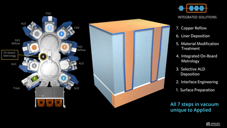
Applied Materials has developed a new materials engineering solution called the Endura® Copper Barrier Seed IMS™. It is an Integrated Materials Solution that combines seven different process technologies in one system under high vacuum: ALD, PVD, CVD, copper reflow, surface treatment, interface engineering and metrology. The combination replaces conformal ALD with selective ALD, eliminating a high-resistivity barrier at the via interface. The solution also includes copper reflow technology that enables void free gap fill in narrow features. Electrical resistance at the via contact interface is reduced by up to 50 percent, improving chip performance and power consumption, and enabling logic scaling to continue to 3nm and beyond. An animation of the process sequence can be viewed at this link: https://bit.ly/3g8HMe1.

“A smartphone chip has tens of billions of copper interconnects, and wiring already consumes a third of the chip’s power,” said Prabu Raja, Senior Vice President and General Manager of the Semiconductor Products Group at Applied Materials. “Integrating multiple process technologies in vacuum allows us to reengineer materials and structures so that consumers can have more capable devices and longer battery life. This unique, integrated solution is designed to accelerate the performance, power and area-cost roadmaps of our customers.”

The Endura Copper Barrier Seed IMS system is now being used by leading foundry-logic customers worldwide. Additional information about the system and other innovations for logic scaling will be discussed at Applied’s 2021 Logic Master Class being held today.

Content Protection by DMCA.com
Tags: Applied MaterialsSemiconductor MaterialsSemiconductors
Semiconductor For You

Semiconductor For You

Browse by Category

  • Aerospace and Defence
  • Articles
  • Automotive
  • Consumer-Electronics
  • Hardware & Software
  • Interview
  • IoT
  • Knowledge Base
  • Lighting
  • Market
  • personal-electronics
  • Power Management
  • Research
  • Semiconductor Events
  • Semiconductor News
  • Technology
  • Wireless
Semiconductor for You

Semiconductor For You is a resource hub for electronics engineers and industrialist. With its blend of
technology features, news and new product information, Semiconductor For You keeps designers and
managers up to date with the fastest moving industry in the world.

Follow Us

Browse by Category

  • Aerospace and Defence
  • Articles
  • Automotive
  • Consumer-Electronics
  • Hardware & Software
  • Interview
  • IoT
  • Knowledge Base
  • Lighting
  • Market
  • personal-electronics
  • Power Management
  • Research
  • Semiconductor Events
  • Semiconductor News
  • Technology
  • Wireless

Recent News

New SPI Absolute Encoder Supports 9 mm to 15.875 mm Motor Shafts

New SPI Absolute Encoder Supports 9 mm to 15.875 mm Motor Shafts

June 11, 2025
Infineon Secures the Future with 10 Billion Integrity Guard Chips Delivered

Infineon Secures the Future with 10 Billion Integrity Guard Chips Delivered

June 11, 2025
  • About
  • Advertise
  • Privacy & Policy
  • Contact

© 2022 Semiconductor For You

No Result
View All Result
  • Home
  • Semiconductor News
  • Technology
    • IoT
    • Wireless
    • Power Management
    • Automotive
    • Hardware & Software
  • Market
  • Knowledge Base
  • Tools
    • Resistor Color Code Calculator

© 2022 Semiconductor For You