• Home
  • About Us
  • Contact Us
Semiconductor for You
  • Home
  • Semiconductor News
  • Technology
    • Automotive
    • Consumer Electronics
    • IoT
    • Lighting
    • Power Management
    • Wireless
    • Personal Electronics
    • Hardware & Software
    • Research
    • Medical Electronics
    • Embedded Design
    • Aerospace & Defence
    • Artificial Intelligence
  • DIY Projects
  • Market
  • Industries
    • Renesas Electronics
  • Knowledge Base
  • Events
  • Tools
    • Resistor Color Code Calculator
No Result
View All Result
Semiconductor for You
No Result
View All Result
Home Knowledge Base

CD4011 NAND Gate : Pin Configuration & Its Applications

Bhushan Chaudhary by Bhushan Chaudhary
August 20, 2022
in Knowledge Base
0
ADVERTISEMENT
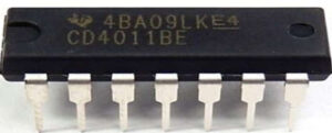
  • The CD4011 is a two-input NAND gate integrated circuit. It is a quadrable NAND gate integrated circuit, which means that it contains four NAND gates in a single package. It is built with CMOS logic.
  • The CMOS logic voltage level is used to design all inputs and outputs. It is used to execute NAND logic, but it can also perform ‘AND A= X x Y’ or ‘OR B = X+Y’ operations using a combination of four gates. NAND’s logical inputs and outputs. For throughput, I/O pins are buffered.
  • CD4011 packages are available in 14-lead hermetic dual-in-line ceramic (F3A suffix), 14-lead dual-in-line plastic (E suffix), 14-lead small-outline (M, MT, M96, and NSR suffixes), and 14-lead thin shrink small-outline configurations (PWR suffix). CD4011s are also available in 14-lead thin shrink small-outline packages (PW suffix).
Practical CD4011 NAND Gate
  • D4011 NAND gates supplement the existing family of CMOS gates by providing the system designer with direct implementation of the NAND function.
  • Now before we jump to the pin configurations and applications, first of all, let us understand what is a NAND gate and what functions does it serve?
  • A NAND Gate is the logic gate that is the inverse of an AND gate. It is a common logic gate that is made up of AND and NOT gates. It is known as a “universal” gate in Boolean algebra because it can produce all other logic gates.
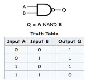
  • A NAND gate is made up of one or more inputs and a single output. The NAND gate’s output is always logic 1 and only goes to logic 0 when all of the NAND gate’s inputs are logic 1. In other words, the NAND gate’s output is always true if at least one of its inputs is false.

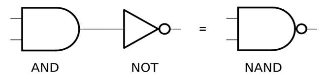
  • The NAND gate function is also known as the Sheffer Stroke function. If all of the NAND gate’s inputs are true, the output is false. It is represented by a symbol that looks like an AND gate with a circle on top, also known as an “inversion circle.”, as shown below.
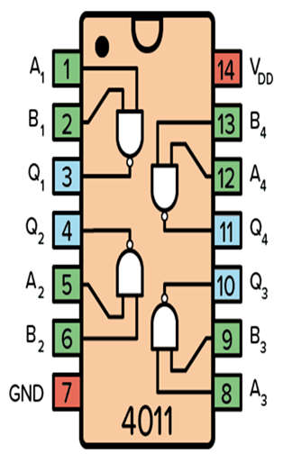
Pin Configuration

Pin Diagram : CD4011 NAND Gate IC
Pin Name Pin No. Type Description
VDD 14 Power Supply Voltage (+3 to +15V)
GND 7 Power Ground (0V)
B1 to B4 2,6,9,13 Input Inputs B of the four NAND gates
Q1 to Q4 3,4,10,11 Output Outputs from the four NAND gates

Features of CD4011 NAND Gate

  • NAND Gate with Dual Input – Quad Package.
  • 5V is the typical operating voltage.
  • 1.5 mA is the high-level output current.
  • 1.5mA is the low-level output current.
  • Propagation Delay: 60 ns.
  • Temperature range of operation: 55 C to + 125 C.
  • 14-pin PDIP, GDIP, and PDSO packages are available.

Applications of CD4011 NAND Gate

  • AV Receivers.
  • Portable Audio Docks.
  • Blu-Ray Players.
  • Home Theater.
  • MP3 Players or Recorders.
  • Personal Digital Assistants (PDAs).
Content Protection by DMCA.com
Bhushan Chaudhary

Bhushan Chaudhary

Browse by Category

  • Aerospace and Defence
  • Articles
  • Automotive
  • Consumer-Electronics
  • Hardware & Software
  • Interview
  • IoT
  • Knowledge Base
  • Lighting
  • Market
  • personal-electronics
  • Power Management
  • Research
  • Semiconductor Events
  • Semiconductor News
  • Technology
  • Wireless
Semiconductor for You

Semiconductor For You is a resource hub for electronics engineers and industrialist. With its blend of
technology features, news and new product information, Semiconductor For You keeps designers and
managers up to date with the fastest moving industry in the world.

Follow Us

Browse by Category

  • Aerospace and Defence
  • Articles
  • Automotive
  • Consumer-Electronics
  • Hardware & Software
  • Interview
  • IoT
  • Knowledge Base
  • Lighting
  • Market
  • personal-electronics
  • Power Management
  • Research
  • Semiconductor Events
  • Semiconductor News
  • Technology
  • Wireless

Recent News

TDK introduces automotive power-over-coax inductor for filters with industry-leading simplicity and efficiency

TDK introduces automotive power-over-coax inductor for filters with industry-leading simplicity and efficiency

June 17, 2025
Mouser Electronics Gears Up for the 6th Edition of India IoT Technical Roadshow

Mouser Electronics Gears Up for the 6th Edition of India IoT Technical Roadshow

June 17, 2025
  • About
  • Advertise
  • Privacy & Policy
  • Contact

© 2022 Semiconductor For You

No Result
View All Result
  • Home
  • Semiconductor News
  • Technology
    • IoT
    • Wireless
    • Power Management
    • Automotive
    • Hardware & Software
  • Market
  • Knowledge Base
  • Tools
    • Resistor Color Code Calculator

© 2022 Semiconductor For You