
Introduction
The Charge Coupled Device (CCD) is an important electronic component used for capturing and processing images. It was invented in 1969 by Willard Boyle and George E. Smith at AT&T Bell Laboratories. CCD technology plays a crucial role in digital imaging systems such as cameras, telescopes, and scanners.
Definition
A Charge Coupled Device (CCD) is a semiconductor device that transfers electrical charge from one location to another within the device. It works like a shift register, where the charge is moved step-by-step and converted into digital signals for processing and storage.
Initially, charge had to be injected manually into the CCD. Later, it was discovered that photoelectric sensors could generate charge when exposed to light. This innovation enabled CCDs to convert analog signals into digital form, making them widely used in imaging devices.
Working Principle of CCD
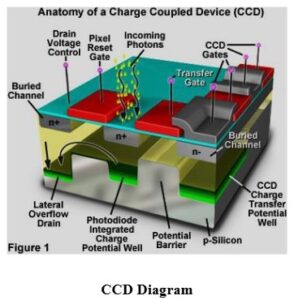
CCD works by converting light into electrical signals and then into digital data. When light falls on the sensor, it generates charge in the form of electrons. These charges are stored in capacitive elements and transferred sequentially across the device.
The movement of charge is controlled in such a way that it can be read, digitized, and stored as image data. This process allows CCDs to capture high-quality images with excellent clarity.
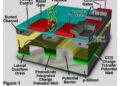
Structure and Operation of CCD
A CCD is mainly divided into two important regions:
1. Photoactive Region
The photoactive region consists of an array of capacitors that capture light and convert it into electrical charge. Depending on the application, this array can be:
- 1D Array: Used in line-scan cameras to capture a single line of an image.
- 2D Array: Used in video and imaging applications to capture full images.
This region is typically made using a silicon layer with appropriate doping to allow efficient charge generation and transfer. Photogenerated charges move through defined channels within the device.
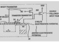
2. Transmission Region
The transmission region is responsible for transferring the generated charge across the device. Once light is captured, control circuits activate the transfer process.
- Charges are moved through a shift register
- Each signal is converted into a voltage
- The signals are then sampled, digitized, and stored
There are different types of CCD operation methods, including:
- Frame Transfer CCD: Transfers the entire image frame for processing using gate control signals.
- Peristaltic CCD: Uses electric fields to move charge efficiently across the device.
CCD Image Formation
When photons strike the CCD sensor, electrons are generated and stored in pixels. The number of electrons corresponds to the intensity of light, which determines the brightness of each pixel in the final image.
Applications of CCD
Astronomy
CCD sensors are widely used in astronomy due to their high sensitivity and linear response to light. They are used in ultraviolet and infrared imaging. Techniques such as drift scanning and noise reduction methods help improve image quality.
Digital Cameras
CCD technology is used in digital cameras to capture high-quality images. Advanced systems like 3CCD cameras improve color accuracy and image clarity by separating light into different color components.
Scientific Imaging
CCDs are used in laboratories and research applications for precise image capture and analysis.
Medical Imaging
CCD sensors are also used in medical devices to capture detailed images for diagnosis and treatment.
Advantages of CCD
- High image quality and resolution
- Excellent sensitivity to light
- Low noise compared to other sensors
- Accurate color reproduction
Limitations of CCD
- Higher power consumption
- More expensive compared to CMOS sensors
- Slower processing speed in some applications
Conclusion
The Charge Coupled Device (CCD) is a powerful technology used in imaging systems across various fields such as astronomy, photography, and medicine. Its ability to convert light into high-quality digital images makes it an essential component in modern electronic devices. Despite some limitations, CCD technology continues to play a vital role in advanced imaging applications.