• Home
  • About Us
  • Contact Us
Semiconductor for You
  • Home
  • Semiconductor News
  • Technology
    • Automotive
    • Consumer Electronics
    • IoT
    • Lighting
    • Power Management
    • Wireless
    • Personal Electronics
    • Hardware & Software
    • Research
    • Medical Electronics
    • Embedded Design
    • Aerospace & Defence
    • Artificial Intelligence
  • DIY Projects
  • Market
  • Industries
    • Renesas Electronics
  • Knowledge Base
  • Events
  • Tools
    • Resistor Color Code Calculator
No Result
View All Result
Semiconductor for You
No Result
View All Result
Home Semiconductor News

InnovationLab demonstrates breakthrough PCB production method based on additive manufacturing

Semiconductor For You by Semiconductor For You
August 4, 2022
in Semiconductor News
0
ADVERTISEMENT

A sustainable and cost-efficient solution to replace etching processes

Heidelberg, Germany – August 4, 2022 – InnovationLab, the expert in printed electronics “from lab to fab”, announces it has achieved a breakthrough in additive manufacturing of printed circuit boards (PCBs), helping meet higher environmental standards for electronics production while also reducing costs.

Within the research project SmartEEs2, funded by Horizon 2020, InnovationLab and its partner ISRA have developed a novel manufacturing process for copper-based solderable circuits. The circuits are screen printed and are compatible with conventional reflow processes.

Producing printed electronics is an additive process that does not use toxic etchants, and runs at comparatively low temperatures of around 150ºC, thus reducing energy consumption. Moreover, the substrates used in additive PCB manufacturing are up to 15 times thinner, compared to conventional techniques, which reduces material consumption and means the production process has less waste.

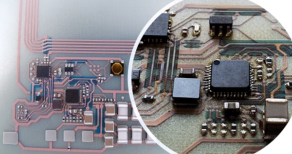
InnovationLab has so far produced a physical prototype, which includes all the important blocks of a smart label. It uses a copper ink to ensure high conductivity. Component mounting can be done in a conventional reflow soldering process, which enables manufacturers to switch to the new technology without investment in new equipment.

Multilayer layer printing, metal and dielectric, was used to produce the target functionality: a low power temperature sensor and logger, an NFC communication interface via a printed antenna, and a compact battery that is charged from a printed solar cell, making the device completely self-sufficient. The new process can produce both standard and flexible PCBs with up to four layers and can be used in product and process development for hybrid electronics.

Dr. Janusz Schinke, Head of Printed Electronics at InnovationLab, said, “This is a state-of-the-art production process, which will decrease costs and reduce logistical dependencies on suppliers, while delivering three key benefits for the environment: consuming fewer materials, using less energy, and producing less waste. By the end of this year, we expect to have scaled this process to high volumes, meeting customer demands of a million solderable tracks or more.”

SmartEEs2 is a European project, which is funded by the European Union’s Horizon 2020 research and innovation program. Its objective is to provide acceleration support to innovative companies for the integration of flexible and wearable electronics technologies, and thus to help European industry’s competitiveness.

Content Protection by DMCA.com
Tags: pcb design
Semiconductor For You

Semiconductor For You

Browse by Category

  • Aerospace and Defence
  • Articles
  • Automotive
  • Consumer-Electronics
  • Hardware & Software
  • Interview
  • IoT
  • Knowledge Base
  • Lighting
  • Market
  • personal-electronics
  • Power Management
  • Research
  • Semiconductor Events
  • Semiconductor News
  • Technology
  • Wireless
Semiconductor for You

Semiconductor For You is a resource hub for electronics engineers and industrialist. With its blend of
technology features, news and new product information, Semiconductor For You keeps designers and
managers up to date with the fastest moving industry in the world.

Follow Us

Browse by Category

  • Aerospace and Defence
  • Articles
  • Automotive
  • Consumer-Electronics
  • Hardware & Software
  • Interview
  • IoT
  • Knowledge Base
  • Lighting
  • Market
  • personal-electronics
  • Power Management
  • Research
  • Semiconductor Events
  • Semiconductor News
  • Technology
  • Wireless

Recent News

New SPI Absolute Encoder Supports 9 mm to 15.875 mm Motor Shafts

New SPI Absolute Encoder Supports 9 mm to 15.875 mm Motor Shafts

June 11, 2025
Infineon Secures the Future with 10 Billion Integrity Guard Chips Delivered

Infineon Secures the Future with 10 Billion Integrity Guard Chips Delivered

June 11, 2025
  • About
  • Advertise
  • Privacy & Policy
  • Contact

© 2022 Semiconductor For You

No Result
View All Result
  • Home
  • Semiconductor News
  • Technology
    • IoT
    • Wireless
    • Power Management
    • Automotive
    • Hardware & Software
  • Market
  • Knowledge Base
  • Tools
    • Resistor Color Code Calculator

© 2022 Semiconductor For You