

Introduction
JTAG (Joint Test Action Group) is a well-known IEEE 1149.1 standard developed in the 1980s to address manufacturing and testing issues in electronic boards and printed circuit boards (PCBs). As electronic components became more compact and complex, physical test access to circuit nodes decreased. To overcome this limitation, boundary scan technology was introduced, leading to the establishment of the JTAG standard.
With the growing complexity of modern electronics, JTAG has become the most widely accepted testing and debugging standard for compact and highly integrated electronic systems. This article explains the JTAG protocol, its working principle, architecture, timing, and applications.
What is JTAG?
JTAG is the common name for the IEEE 1149.1 Standard Test Access Port (TAP) and Boundary Scan Architecture developed by the Joint Test Action Group. Since Intel introduced the first processor with JTAG support, this boundary scan architecture has been widely adopted in computer processors, microcontrollers, FPGAs, and CPLDs.


The IEEE 1149.1 standard defines a method for testing the interconnections and internal logic of integrated circuits to ensure proper functionality after manufacturing. It allows testing of solder joints and PCB connections without physical probing.
JTAG Pin Configuration
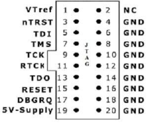

The JTAG interface typically uses a 20-pin connector. Each pin and its function are described below:
- Pin 1 (VTref): Target reference voltage used to sense the target power supply (1.5V to 5.0V DC).
- Pin 2 (Vsupply): Target supply voltage (1.5V to 5.0V DC).
- Pin 3 (nTRST): Test reset pin used to reset the TAP controller state machine.
- Pins 4, 6, 8, 10, 12, 14, 16, 18, 20: Ground (GND) pins.
- Pin 5 (TDI): Test Data In pin used to shift data into the target device.
- Pin 7 (TMS): Test Mode Select pin used to control TAP controller state transitions.
- Pin 9 (TCK): Test Clock pin that synchronizes TAP controller operations.
- Pin 11 (RTCK): Return TCK pin used for adaptive clocking.
- Pin 13 (TDO): Test Data Out pin used to shift data out of the target device.
- Pin 15 (nSRST): Target system reset pin.
- Pins 17 and 19: Not connected (NC).
Working of JTAG
JTAG was originally designed for boundary testing of printed circuit boards. A typical PCB may contain several integrated circuits such as CPUs, FPGAs, and memory devices interconnected through numerous signal lines.
Using JTAG, all output pins of one device (for example, a CPU) and input pins of another device (such as an FPGA) can be controlled and monitored. Test data is transmitted from one device and received by another, verifying the integrity of PCB interconnections.
The JTAG interface consists of four mandatory signals: TDI, TDO, TMS, and TCK. These signals are connected in a specific manner. TMS and TCK are connected in parallel to all JTAG-enabled devices, while TDI and TDO are connected in series to form a scan chain.
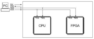

Each JTAG-compliant IC includes four JTAG pins, with an optional TRST pin. Typically, these pins are dedicated exclusively to JTAG functionality. Today, JTAG is widely used not only for boundary testing but also for FPGA configuration, in-system programming, and on-chip debugging.


JTAG Architecture
The JTAG architecture includes a serial scan path known as the Boundary Scan Register (BSR). This register contains multiple boundary scan cells placed between the core logic and the I/O pins of the device.
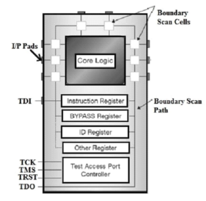

The JTAG interface uses a Test Access Port (TAP) with the following signals:
- TCK: Synchronizes internal state machine operations.
- TMS: Determines the next state of the TAP controller.
- TDI: Shifts data into the device.
- TDO: Shifts data out of the device.
- TRST: Optional signal to reset the TAP controller.
TAP Controller
The TAP controller is the core of the JTAG architecture. It consists of a state machine, an instruction register, and multiple data registers. The TAP controller reads the TMS and TCK signals to determine the current operation mode.
The TAP controller supports two primary modes: instruction mode and data mode. The data input pin loads data into boundary scan cells or registers, while the data output pin retrieves data from them.
JTAG Registers
JTAG-compliant devices contain one instruction register and at least two data registers.
Instruction Register
The instruction register stores the current instruction that defines which data register is selected and how the test data is processed.
Data Registers
The main data registers include:
- Boundary Scan Register (BSR): Used for testing and controlling I/O pins.
- BYPASS Register: A single-bit register that bypasses the device to reduce scan chain length.
- IDCODE Register: Stores the device identification code and revision number.
The IDCODE register helps link the device to its BSDL (Boundary Scan Description Language) file, which contains boundary scan configuration details.
Difference Between JTAG and UART
| JTAG | UART |
|---|---|
| Synchronous interface | Asynchronous interface |
| Used for testing, debugging, and programming | Used for serial communication |
| Uses TDI, TDO, TMS, TCK, and TRST | Uses TX and RX lines |
| Mainly used in processors, FPGAs, and CPLDs | Mainly used for device-to-device communication |
JTAG Protocol Analyzer
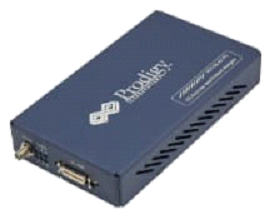

A JTAG protocol analyzer is used to capture and analyze communication between a host and a device under test. These analyzers can operate as JTAG masters or slaves, generate JTAG traffic, and decode protocol packets.
Features
- Supports JTAG frequencies up to 25 MHz
- Simultaneous protocol generation and decoding
- Variable data speed and duty cycle
- User-defined TDI and TCK delays
- USB 2.0 or 3.0 host interface
- Protocol timing diagram analysis
- Continuous data streaming
JTAG Timing Diagram
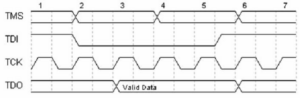

In JTAG timing, the TDO pin remains in a high-impedance state except during Shift-IR and Shift-DR states. During these states, TDO is updated on the falling edge of TCK and sampled on the rising edge. TDI and TMS are sampled on the rising edge of TCK by the target device and updated on the falling edge by the host.
Applications of JTAG
- Processor debugging and emulation
- FPGA and CPLD programming
- PCB testing without physical probes
- Board-level manufacturing tests
- In-system programming
- Fault diagnosis and debugging