• Home
  • About Us
  • Contact Us
Semiconductor for You
  • Home
  • Semiconductor News
  • Technology
    • Automotive
    • Consumer Electronics
    • IoT
    • Lighting
    • Power Management
    • Wireless
    • Personal Electronics
    • Hardware & Software
    • Research
    • Medical Electronics
    • Embedded Design
    • Aerospace & Defence
    • Artificial Intelligence
  • DIY Projects
  • Market
  • Industries
    • Renesas Electronics
  • Knowledge Base
  • Events
  • Tools
    • Resistor Color Code Calculator
No Result
View All Result
Semiconductor for You
No Result
View All Result
Home Semiconductor News

Monolithic 3D Shows Promise, Challenges

Semiconductor For You by Semiconductor For You
October 23, 2017
in Semiconductor News
0
ADVERTISEMENT

BURLINGAME, Calif. — Monolithic 3D integration shows promise as a way to create faster, cheaper, smaller chips. But despite interest from several quarters, most efforts are still in a research stage with significant work ahead in proving the technology and building an ecosystem for it.

That was the take away from the annual S3S conference here where ARM, CEA-Leti, DARPA, Mentor Graphics and Qualcomm presented work in the field. M3D aims to carve diverse functions into blocks stacked vertically in one or more die, however most approaches have not yet demonstrated commercial viability.

The Leti European research insitute has worked for several years on Cool Cube, an approach for vertically stacking transistors. IBM, Qualcomm and STMicroelectronics are among Leti’s partners on the project. While it holds promise, it has yet to show how it can scale to problems such as global routing in a full M3D chip.

A Qualcomm research director co-hosted a half-day program on Cool Cube here. His enthusiasm for the area which he named 3D VLSI was clear, as was the vigor with which he is still exploring many shortcomings of current approaches.

Years ago, Qualcomm was equally vigorous exploring through silicon vias (TSVs), an approach many thought would be used for mobile application processors. But today, Qualcomm has largely dropped that effort because the thermal and cost challenges for TSVs in such chips remain largely unsolved. Meanwhile TSMC and others have made advances in wafer-level fan-out packaging now used in Apple’s iPhone processors

Startup MonolithIC3D has been championing M3D with its CEO, semiconductor veteran Zvi Or-Bach, acting as an organizer for the event. The five-person company with Or-Bach as its only full-time employee is said to have compelling ideas and IP for M3D, but it has yet to find a partner to test them in silicon.

DARPA sees M3D as one of many promising efforts to reinvigorate the chip industry at a time when it is seeing slowing gains and rising costs. One of six DARPA programs on next-generation silicon design will explore chip stacks, and some companies have said they will proposed M3D projects for it.

Top challenges for M3Ds include:

  • Getting EDA giants to build design tools for it
  • Protecting components from high temperatures required to make some elements in a device
  • Aligning circuits with transistor-level accuracy
  • Routing dozens if not hundreds of elements
  • Reducing costs of layering memory and logic in a single device

Still M3D has potential, said Nathan Brookwood, market watcher at Insight64 who attended a Cool Cube workshop here.

“It’s like going upstairs and downstairs rather than from one end of a building to the other on the same floor. Instead of travelling tens of millimeters across a chip from a cache to a computing element, you could just go up one or two millimeters,” he said.
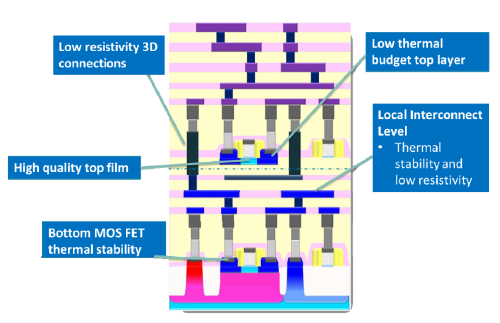
Leti preps an M3D multi-project wafer

Leti gave a frank rundown of challenges for M3D in general and its Cool Cube approach specifically. Click to enlarge. (Image: Leti)

Content Protection by DMCA.com
Semiconductor For You

Semiconductor For You

Browse by Category

  • Aerospace and Defence
  • Articles
  • Automotive
  • Consumer-Electronics
  • Hardware & Software
  • Interview
  • IoT
  • Knowledge Base
  • Lighting
  • Market
  • personal-electronics
  • Power Management
  • Research
  • Semiconductor Events
  • Semiconductor News
  • Technology
  • Wireless
Semiconductor for You

Semiconductor For You is a resource hub for electronics engineers and industrialist. With its blend of
technology features, news and new product information, Semiconductor For You keeps designers and
managers up to date with the fastest moving industry in the world.

Follow Us

Browse by Category

  • Aerospace and Defence
  • Articles
  • Automotive
  • Consumer-Electronics
  • Hardware & Software
  • Interview
  • IoT
  • Knowledge Base
  • Lighting
  • Market
  • personal-electronics
  • Power Management
  • Research
  • Semiconductor Events
  • Semiconductor News
  • Technology
  • Wireless

Recent News

Infineon advances on 300-millimeter GaN manufacturing roadmap as leading Integrated Device Manufacturer (IDM)

Infineon advances on 300-millimeter GaN manufacturing roadmap as leading Integrated Device Manufacturer (IDM)

July 2, 2025

₹1 Lakh Cr RDI Scheme Approval

July 2, 2025
  • About
  • Advertise
  • Privacy & Policy
  • Contact

© 2022 Semiconductor For You

No Result
View All Result
  • Home
  • Semiconductor News
  • Technology
    • IoT
    • Wireless
    • Power Management
    • Automotive
    • Hardware & Software
  • Market
  • Knowledge Base
  • Tools
    • Resistor Color Code Calculator

© 2022 Semiconductor For You