
What is MOSFET?
MOSFET (Metal Oxide Semiconductor Field Effect Transistor) is a three-terminal, voltage-controlled transistor.
The voltage applied to the gate terminal controls the current flowing from the source to the drain.
It is also known as IGFET (Insulated Gate Field Effect Transistor).
The three main terminals of a MOSFET are:
- Source (S)
- Gate (G)
- Drain (D)
MOSFETs are commonly used for switching and amplifying electronic signals.
Types of MOSFET
- Enhancement Type MOSFET
- Depletion Type MOSFET


Enhancement Mode MOSFET
- N-Channel Enhancement MOSFET
- P-Channel Enhancement MOSFET
Depletion Mode MOSFET
- N-Channel Depletion MOSFET
- P-Channel Depletion MOSFET
Construction of MOSFET
A MOSFET actually has four terminals: Source, Gate, Drain, and Body (also called Substrate).
The body terminal is usually internally connected to the source, so it is often not shown externally.
The gate terminal is metallic and separated from the semiconductor by a thin dielectric layer of SiO₂.
This insulated structure allows the gate voltage to control channel formation without any direct conduction.
N-Channel Enhancement MOSFET
In an N-channel Enhancement MOSFET, the source and drain are heavily doped N-type regions, while the substrate is P-type.

Electrons are the majority charge carriers. The source and drain are physically separated, and a channel forms only when a positive gate voltage is applied.
P-Channel Enhancement MOSFET
In this MOSFET, the source and drain are heavily doped P-type regions, and the substrate is N-type. Holes are the majority charge carriers.

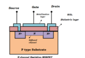
N-Channel Depletion MOSFET
In an N-channel Depletion MOSFET, an N-type semiconductor strip connects the source and drain. The substrate is P-type. Current flows even without any gate voltage. Applying a negative gate voltage repels electrons, reducing the drain current, hence putting the MOSFET in depletion mode.
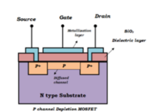
P-Channel Depletion MOSFET
Here, a P-type semiconductor strip connects the source and drain. The substrate is N-type, and holes are the majority carriers. Applying a positive gate voltage reduces the current by repelling holes.
Working of MOSFET
Working of N-Type Depletion MOSFET
There is no PN junction between the gate and channel. The gate, dielectric (SiO₂), and semiconductor form a parallel plate capacitor. When a negative voltage is applied to the gate, holes are attracted toward the oxide layer while electrons are repelled. This reduces the number of free electrons in the channel, causing the drain current (ID) to decrease. The more negative the gate voltage, the lower the drain current.
Working of N-Type Enhancement MOSFET
When a positive gate voltage is applied, electrons are attracted toward the oxide layer, forming a conductive channel. This increases the drain current (ID). A higher positive gate voltage enhances the channel further and increases current flow — hence the name Enhancement Mode.
Working of P-Type MOSFET (PMOS)
A lightly doped N-type substrate contains two heavily doped P+ regions acting as source and drain. When the gate voltage is more negative than the drain-source voltage (VDD), holes flow more easily, and the PMOS operates in Enhancement Mode.
When the gate voltage is more positive, holes are repelled, reducing current flow. This puts the PMOS in Depletion Mode.
Thus, by changing the gate voltage polarity, both NMOS and PMOS can operate in either Enhancement or Depletion modes.