
Introduction
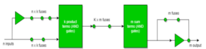
A Programmable Logic Array (PLA) is a type of logic device used to implement combinational logic circuits. It consists of programmable AND and OR gate planes, which can be interconnected to produce desired logical outputs. A PLA typically has 2N AND gates for N input variables and M OR gates for M outputs. This structure allows the realization of various logic functions in the Sum of Products (SOP) form.
PLAs differ from Programmable Array Logic (PAL) and Generic Array Logic (GAL) devices because both the AND and OR planes in a PLA are programmable. This provides greater flexibility but increases design complexity.
Block Diagram of a PLA
A PLA is conceptually similar to a Read Only Memory (ROM), but unlike ROM, it does not provide full variable decoding and does not generate all minterms. Despite being called “programmable,” it does not require software programming like C or C++; instead, its interconnections are configured at the hardware level.
Example Truth Table
| A | B | C | F1 | F2 |
|---|---|---|---|---|
| 0 | 0 | 0 | 0 | 0 |
| 0 | 0 | 1 | 0 | 0 |
| 0 | 1 | 0 | 0 | 0 |
| 0 | 1 | 1 | 0 | 1 |
| 1 | 0 | 0 | 1 | 0 |
| 1 | 0 | 1 | 0 | 1 |
| 1 | 1 | 0 | 1 | 0 |
| 1 | 1 | 1 | 1 | 1 |
Boolean Equations
F1 = AB’C’ + ABC’ + ABC
On simplifying: F1 = AB + AC’
F2 = A’BC + AB’C + ABC
On simplifying: F2 = BC + AC
These functions can be implemented using a PLA circuit that connects AND gates and OR gates in a programmable manner to produce the required outputs.
Design of Programmable Logic Array (PLA)
A PLA represents Boolean functions in the Sum of Products (SOP) form. The device is designed using logic gates such as AND, OR, and NOT, all fabricated on a single chip. Every input variable and its complement are accessible to each AND gate.
The outputs of AND gates are connected to the inputs of OR gates, and the final outputs of the PLA are generated by the OR gates. Since both the AND and OR connections are programmable, a PLA provides high flexibility but is generally more complex and costly compared to PAL devices.
In practical PLAs, fuses are often used at the intersection points between AND and OR planes. Unnecessary connections can be removed by blowing the fuses, creating a custom interconnection pattern suitable for the required logic design.
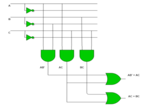
Example: Implementing Boolean Expressions Using PLA
Use a PLA to implement the following Boolean functions:
X = AB + AC’
Y = AB’ + BC + AC’
Both expressions are in SOP form. The common product term AC’ appears in both functions, reducing hardware complexity. The required configuration uses 4 AND gates and 2 OR gates.
Each AND gate can accept both the normal and complemented forms of the input variables (A, A’, B, B’, C, C’).
The output OR gates combine the desired product terms using programmable connections.
Common PLA and FPLA ICs
| IC No. | Type | Inputs | Outputs | Packaging |
|---|---|---|---|---|
| 82S200 | PLA | 16 | 8 | 28-pin DIP |
| 82S201 | PLA | 16 | 8 | 28-pin DIP |
| 82S100 | FPLA | 16 | 8 | 28-pin DIP |
| 82S101 | FPLA | 16 | 8 | 28-pin DIP |
| DM7575 | PLA | 14 | 8 | 24-pin DIP |
| DM7576 | PLA | 14 | 8 | 24-pin DIP |
Advantages of PLA
- Highly efficient for implementing combinational logic circuits.
- Provides flexibility with programmable AND and OR arrays.
- Low power consumption.
- Reliable and durable design.
- Compact structure suitable for large-scale integration.
Conclusion
The Programmable Logic Array (PLA) is a versatile hardware device for implementing combinational logic in digital systems. Its programmable AND and OR planes allow complex logic functions to be realized efficiently, making it an essential component in modern digital circuit design.