
While designing low power system, designer has the choice between choosing low-power components or switching off the power to peripheral devices. When considering the choice of non-volatile flash memories, the designer has these same two options available to them – each of which has its pros and cons from system operation, power consumption and reliability perspectives. However, there is another low power solution available that has the added benefit of simplifying your system design and improving reliability.
Typical design using external flash memory
Despite the proliferation of microcontroller (MCU) devices with embedded flash and a wealth of low-power modes in which they can operate, more and more systems still require an external flash memory device to supplement the on-chip flash for expansion reasons. Over-the-Air (OTA) updates, datalogging, user profiles, and other applications all contribute to this.
For many basic applications, a typical design as shown in Figure 1 is an acceptable solution.
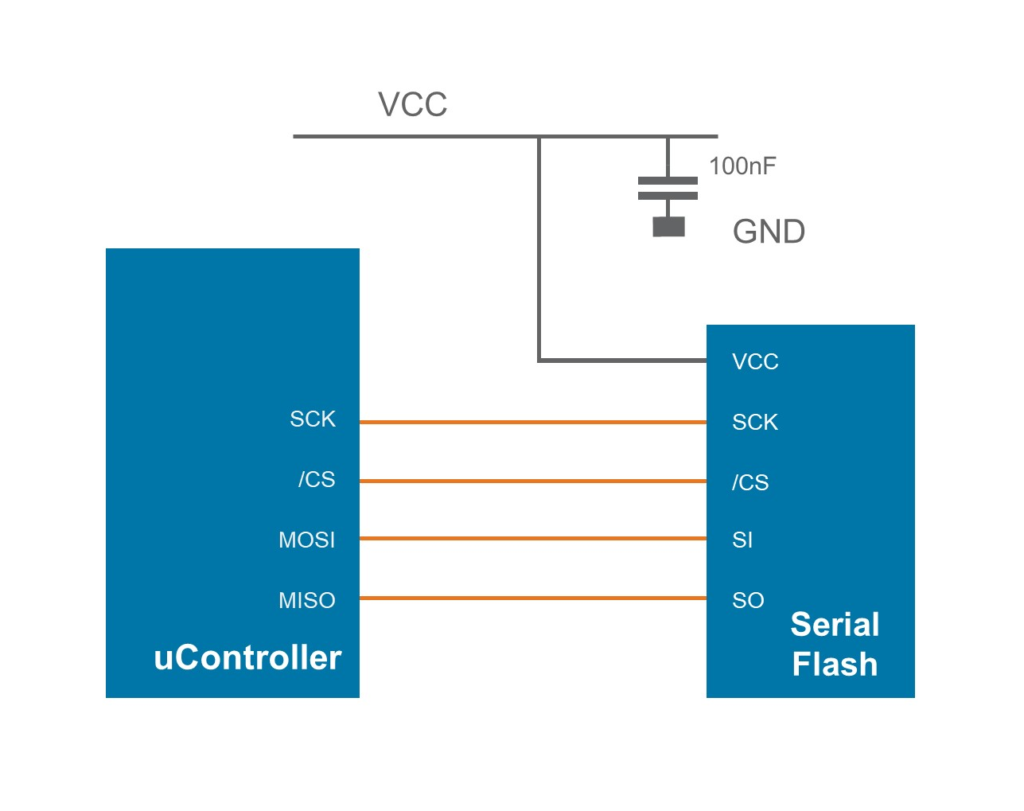
In this solution, the power is continuously supplied to the flash device. When the Serial Flash Chip Select Signal ( /CS ) is not asserted and the memory is in standby mode, standby current is typically about ~10uA to ~20uA. There is also an option to go into the command-driven Deep Power Down mode, which reduces standby power even more to typically ~2uA – ~5uA.
However, in some other systems, such as energy harvesting or small battery powered devices, even 2uA may still represent too high a current consumption value. And, if the flash is accessed infrequently or very rarely used, 2uA standby for extended periods may represent an excessive drain on the power supply and energy reserves – reducing overall battery / system operating life.
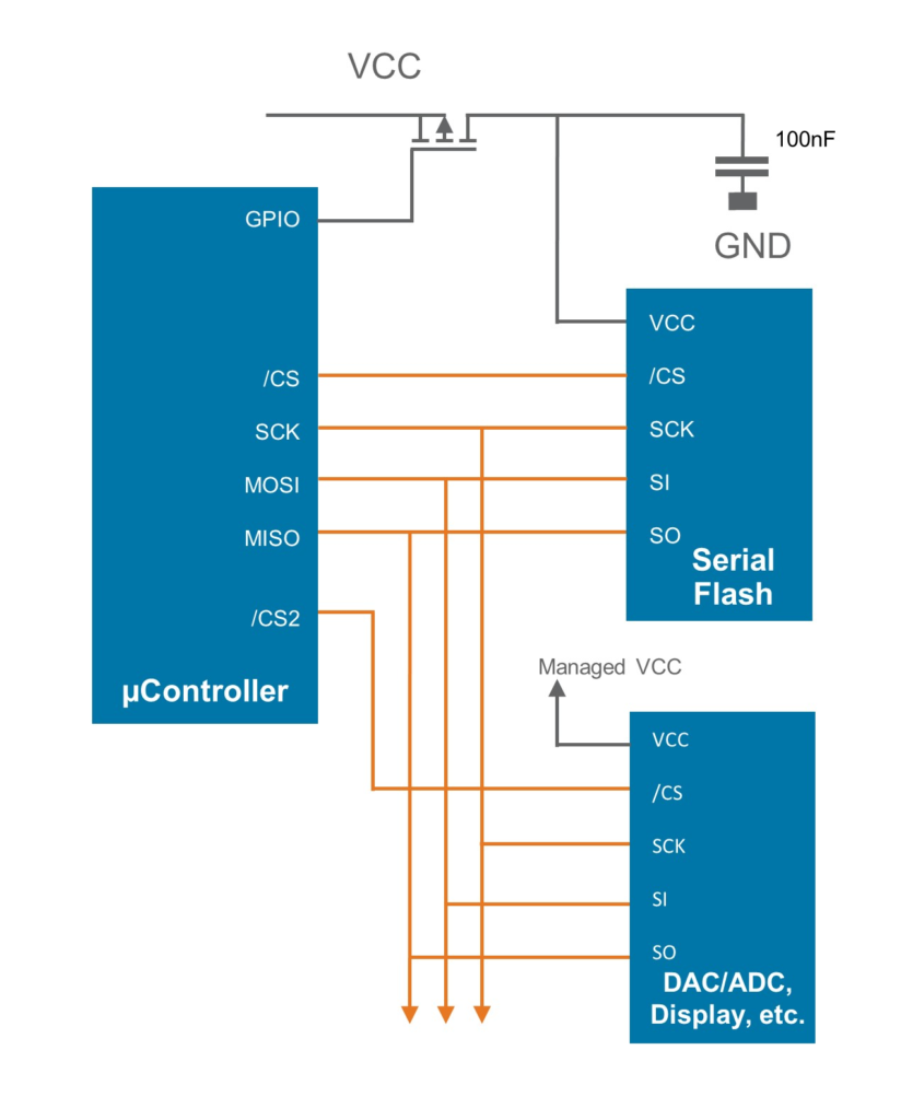
External flash with simple power switching control circuit
To improve the system battery life, designers often implement a simple power switching control circuit as shown in Figure 2. The power to the flash device is managed under software control through a spare MCU GPIO pin so that serial flash is only powered when required.
Don’t get too comfortable!
The inclusion of the MOSFET to completely switch off the serial memory VCC will reduce the standby power of the memory to zero, but the MOSFET itself has a potential leakage current and drain current, in some cases up to 1.5uA, which is only 500nA better than the memory in normal standby at up to 2uA.
Reliability concerns
The solution utilizing an external FET or LDO with control gate to manage power to a peripheral device VCC pin is becoming more common; however, this does also require an extra MCU GPIO pin.
More importantly, care must be taken when multiple peripheral devices share a common SPI bus and where the individual devices have switched VCC pins.
In the configuration shown in Figure 2, if the VCC to the flash is switched off and VCC = 0V, continuing to access the other SPI controlled devices (e.g. DAC/ADC/Display) on the SPI bus will result in bus signals also appearing on the serial flash SPI pins.
In this scenario, the high VCC on peripheral SPI bus pins when VCC for the flash (or other devices) is at zero would result in the I/O protection diodes being forward biased, and the device will potentially draw power through the I/O pins themselves. This could lead to short-term or long-term reliability concerns and operational problems.
For all situations where any other devices that might be powered on while the flash is turned off, stray capacitance should also be minimized so that the voltage on any pin does not exceed the voltage on the VCC pin. Alternatively, the designer could consider a more cumbersome solution and add a separate SPI bus for the serial memory where VCC can be turned off. Careful hardware and software design and implementation can overcome all of these challenges and concerns. However…
The Ultra-Deep Power Down (UDPD) option
…a more efficient solution is achieved by integrating the power control circuitry into the memory device itself and allowing the master device (MCU) to control the power mode through the serial flash SPI command interface. This saves the GPIO pin for other purposes. See the diagram in Figure 3.
Benefits to this solution are:
- It consumes much less power than standard Deep Power Down.
- It does not require an external MOSFET.
- It allows the designer to use the same SPI bus for other peripherals and therefore simplify the design.
- It mitigates reliability concerns as the VCC pin is always connected to VCC, and power is controlled internally.
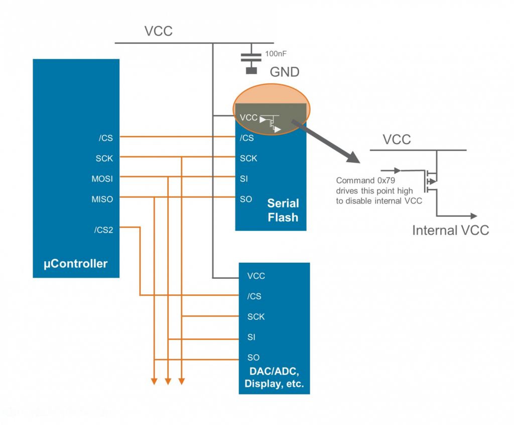
and driven through the SPI command interface
Additional benefits to this solution are:
- It saves a GPIO pin that would be used for switching the external MOSFET or LDO.
- It simplifies the software because it eliminates the surplus MOSFET/LDO control routines.
- It provides for a cleaner PCB design and reduced BoM.
The Adesto Fusion, FusionHD™ (AT25XExxx) and DataFlash™ (AT45DBxxxE/F) flash memory devices offer this Ultra Deep Power Down mode in addition to Standby and Deep Power Down modes. Standby and Deep Power Down modes result in a current consumption similar to or lower than other industry standard flash devices.
The Ultra Deep Power Down mode takes the quiescent current down to less than 200nA for Fusion, 100nA for FusionHD and less than 400nA for DataFlash
Conclusion
Choosing the proper low-power memory can be a critical system design factor for energy harvesting or small battery-powered devices. Understanding and managing the interaction of components on your SPI bus is also essential to improving functionality and reliability. By considering how memory is implemented in real-world systems, Adesto’s serial flash memory solutions offer designers the option to simplify the design, reduce risk, improve reliability and save on external components, greatly simplifying the circuit and reducing bill of materials cost.