• Home
  • About Us
  • Contact Us
Semiconductor for You
  • Home
  • Semiconductor News
  • Technology
    • Automotive
    • Consumer Electronics
    • IoT
    • Lighting
    • Power Management
    • Wireless
    • Personal Electronics
    • Hardware & Software
    • Research
    • Medical Electronics
    • Embedded Design
    • Aerospace & Defence
    • Artificial Intelligence
  • DIY Projects
  • Market
  • Industries
    • Renesas Electronics
  • Knowledge Base
  • Events
  • Tools
    • Resistor Color Code Calculator
No Result
View All Result
Semiconductor for You
No Result
View All Result
Home Knowledge Base

Shockley Diode – Working and Its Applications

Mrudul Ramteke by Mrudul Ramteke
July 21, 2022
in Knowledge Base
0
ADVERTISEMENT
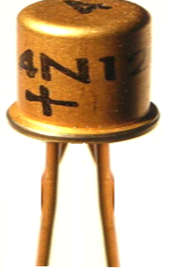
  • Shockley diodes are four-layer PNPN semiconductor devices. It is a two-terminal device that’s why it is characterized as a diode.
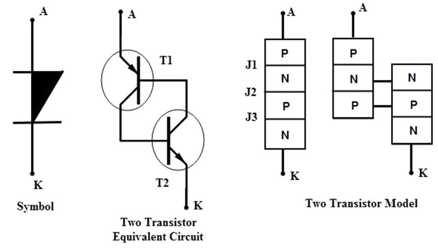
  • These behave as a pair of interconnected PNP and NPN transistors.
  • These diodes are used primarily for switching applications as they can only perform the “ON” or “OFF” function thus, they are classified as a thyristor.
  • This diode was the early invention in thyristor class and was invented by William Bradford Shockley.

Constructions of Shockley Diode

  • The construction of the diode can be done by connecting 4-layers to form a PNPN junction.
  • The equivalent circuit of this diode using two transistors is shown in the above figure where the collector of a transistor T1 is connected to the base of T2.
  • The junction J1 is formed at the emitter-base junction of T1, J2 is at a common connected base-collector junction between T1 and T2,and the J3 is at the base-emitter junction of T2.
  • Therefore, as the base-emitter junctions, J1 and J3 must be forward biased and as a collector base junction, J2 must be reversely biased for linear operation.

Working of Shockley Diode

  • As discussed above, these diodes consist of three junctions J1, J2, and J3. When the voltage is applied to this diode in such a way that the anode is made positive concerning the cathode, junctions J1 and J3 are forward biased and J2 is reverse biased.
  • When the diode is to be operated in forward biasing then J1 and J3 are forward biased and junction J2 is reverse biased. The Shockley diode is operated in forward-biased mode only.
  • When J1 and J3 are reversed biased and J2 is forward biased the devices start operating in reversed biased mode. But when it is operated in reverse biased and the voltage exceeds the breakdown voltage the diode gets damaged. So this diode is operated in forwarding biased mode only.

Advantages of Shockley Diode

  • Reverse voltage can be blocked easily.
  • It can be protected by a fuse from over current.
  • These diodes have a high switching speed.
  • It gets latched into the on-state.
  • It can perform more as compared to a transistor because its construction includes two transistors that are connected through a common terminal.
  • Forward voltage drop is low so power dissipation is also low.

Disadvantages of Shockley Diode

  • It cannot control at a fast speed.
  • Not simple to turn OFF.
  • There is no control above the forward breakdown voltage.
  • It conducts only in a single direction.
  • Its construction is somewhat difficult because it uses four semiconductor material layers.
  • It can switch ON suddenly because of the rate effect.
  • It doesn’t include any controlling terminal.

Applications of Shockley Diode

  • This diode can be used as a trigger switch within the circuits to switch ON an SCR.
  • It can be used in relaxation oscillators.
Content Protection by DMCA.com
Mrudul Ramteke

Mrudul Ramteke

Browse by Category

  • Aerospace and Defence
  • Articles
  • Automotive
  • Consumer-Electronics
  • Hardware & Software
  • Interview
  • IoT
  • Knowledge Base
  • Lighting
  • Market
  • personal-electronics
  • Power Management
  • Research
  • Semiconductor Events
  • Semiconductor News
  • Technology
  • Wireless
Semiconductor for You

Semiconductor For You is a resource hub for electronics engineers and industrialist. With its blend of
technology features, news and new product information, Semiconductor For You keeps designers and
managers up to date with the fastest moving industry in the world.

Follow Us

Browse by Category

  • Aerospace and Defence
  • Articles
  • Automotive
  • Consumer-Electronics
  • Hardware & Software
  • Interview
  • IoT
  • Knowledge Base
  • Lighting
  • Market
  • personal-electronics
  • Power Management
  • Research
  • Semiconductor Events
  • Semiconductor News
  • Technology
  • Wireless

Recent News

New SPI Absolute Encoder Supports 9 mm to 15.875 mm Motor Shafts

New SPI Absolute Encoder Supports 9 mm to 15.875 mm Motor Shafts

June 11, 2025
Infineon Secures the Future with 10 Billion Integrity Guard Chips Delivered

Infineon Secures the Future with 10 Billion Integrity Guard Chips Delivered

June 11, 2025
  • About
  • Advertise
  • Privacy & Policy
  • Contact

© 2022 Semiconductor For You

No Result
View All Result
  • Home
  • Semiconductor News
  • Technology
    • IoT
    • Wireless
    • Power Management
    • Automotive
    • Hardware & Software
  • Market
  • Knowledge Base
  • Tools
    • Resistor Color Code Calculator

© 2022 Semiconductor For You