
Organic based nano-contaminants are a serious defect commonly found in micro-electronics manufacturing processes, including data storage, semiconductor and LED. These kinds of organic contaminants are a serious defectivity problem for Manufacturers because they cause yield problems, and process delays, and they can even lead to scrap product.
The contaminants come from different sources, including wafer transfer and handling, airborne molecular contamination, cleaning techniques, chemical processing and the amount of human interaction with the processes. Significant efforts are being made for the detection and prevention of defects; however, there is still an important class, including organic nanocontaminants, where an exact identification is difficult to achieve using existing instrumentation, due to inadequate resolution or even damage to the sample during measurement.
AFM-IR is a technique that can allow precise chemical identification of contaminants and provide multiple property analysis with nanoscale resolution.
The following are the key capabilities of the AFM-IR technique:
- AFM-IR uniquely and unambiguously identifies organic nano-contaminants on wafers, media and slider substrates
- Simultaneous nanoscale chemical and property mapping information
- Nanoscale IR Spectroscopy directly correlates to FTIR libraries
Organic Nanocontamination of Bare Silicon Wafer
In order to show nanoscale chemical characterization capabilities on the nanoIR2-FS system, contaminated silicon wafers were prepared with known materials typically found in semiconductor fabrication environments and then examined. For each sample, tapping AFM-IR imaging was employed to trace the contaminants, followed by AFM-IR measurements.
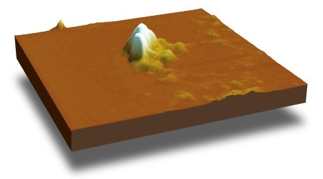
The AFM height image (Figure 1a) shows the thickness variation (20 to 100 nm) of the contaminants that reside (human skin tissue) on the wafer. AFM-IR spectra were then gathered at sites with variable sample thickness (Fig. 1b).
The observed IR intensities varied with sample thickness, as expected. However, the overall signal-to-noise ratio is enough to accurately detect the material, even at 20 nm thickness, reflecting the extraordinary sensitivity in the detection of thin samples.
.jpg)
Figure 1. (a) AFM height image of human skin residue on silicon wafer. (b) Corresponding AFM-IR spectra; Amide I and II bands are indicated.
The nanoIR2-FS’s new FASTspectra capabilities enable quicker acquisition of spectra over the full IR tuning range and allow for a reduction in spectral acquisition time by a factor of 10. As shown in Figure 2, this achievement still allows accurate collection of FTIR spectra.
The AFM-IR spectra obtained from the sample were compared with a common FTIR database (KnowItAll, Bio-Rad Inc.). The ~30 nm tall contamination residue was positively detected as polyethylene terephthalate (PET), a polymer typically used in polyester fabrics.
.jpg)
Figure 2. (a) AFM height image of a wafer with organic residue. (b) FASTspectra data on (red) and off (blue) the contaminant. (c) Positive FTIR database identification of the surface contaminant as PET.