Barley Li, Applications Engineering Manager – Technical Content, APAC, DigiKey
Millimeter wave (mmWave) imaging systems are becoming increasingly common in security operations at public buildings, stadia, and airports. These systems can detect both metallic and non-metallic threats and report their location within the scan area, allowing security professionals to locate and identify suspicious items more quickly. This article will discuss the basics of mmWave imaging, explain how components work together in a mmWave solution designed by Analog Devices, Inc. (ADI), and highlight the role of edge processing in more nimble iterations of the technology.

mmWave 101
In an mmWave system, an array of transmitters and receivers is connected to a spatially dispersed antenna array. At a given point in time, one antenna in the array is transmitting a low-power, single-frequency, omnidirectional radio frequency (RF) signal that reflects off the target (Figure 1). This reflection generates backscattered signals that are received by all the antennas in the array. Integrated circuits (ICs) attached to the antennas measure the phase and amplitude of the received backscatter signals.
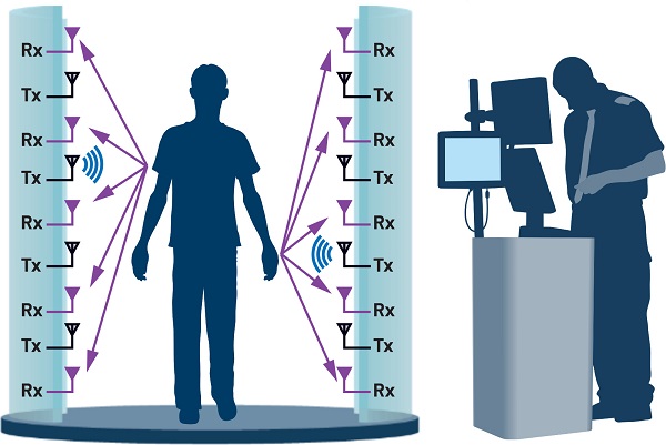
Identical signals are sent from each transmitting antenna sequentially, and the measurement process is repeated for each transmission. Repeating the entire procedure over multiple frequencies between 10 GHz and 40 GHz ensures that the system captures varying RF-signal penetration depth and signal reflections as frequency changes.
Resolution depends on the number of transmit and receive channels. Airport scanners, for instance, have many channels to support the resolution needed to detect small objects like razor blades. A lower channel count in situations where weapons and explosives are the main concerns lowers cost and scanning time.
Processors combine the backscatter information into a matrix of vectors. When the vectors are correlated with frequency and spatial location, the resulting multidimensional array can be used to create an image that can identify both metallic and non-metallic objects that are concealed between and underneath layers of clothing.
The speed of the scan depends on how quickly the system can process backscatter data, switch from transmitter to transmitter, and cycle through the desired frequencies. For example, a system with 500 elements that covers the 10 GHz to 40 GHz range in 50 MHz increments must make 300,000 switches. Fast switching allows today’s deployed mmWave systems to create a useful image when the person being scanned has posed for just a few seconds. With still faster switching times, mmWave systems could detect threats while subjects walk through detectors without pausing.
Building mmWave systems
To detect potential threats, achieve the desired resolution, and facilitate quick scanning, mmWave system designers must select hardware that works in tandem. ADI’s integrated mmWave system solution includes an ADF4368 microwave wideband synthesizer, multiple ADAR2001 transmitter ICs, multiple ADAR2004 receiver ICs, and AD9083 analog-to-digital converters (ADCs), each of which will be discussed in turn below (Figure 2).
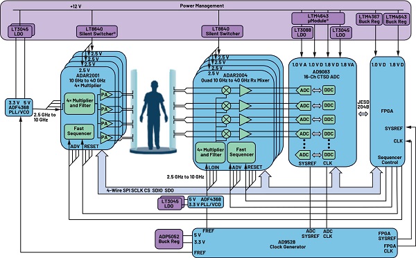
The signal chain begins with the ADF4368 microwave wideband phase-locked loop (PLL) synthesizer with integrated voltage-controlled oscillator (VCO) (Figure 3). The ADF4368 generates frequency steps from 2.5 GHz to 10 GHz in 12.5 GHz increments, well within its 800 MHz to 12.8 GHz range. The continuous wave (CW), single-ended RF signals have jitter under 30 fsecRMS.
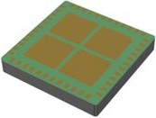
Figure 3: The ADF4368 microwave wideband synthesizer with integrated VCO supplies low jitter CW RF outputs over the 2.5-GHz-to-10-GHz frequency range. (Image source: Analog Devices, Inc.)
The ADF4368 outputs signals with 9 dBm (7.94 mW) power. Because the transmitter ICs need much less power, ADF4368 outputs can be split seven times, driving up to 128 4-channel transmitter ICs or 512 channels.
The ADAR2001 transmitter ICs (Figure 4) accept input from the ADF4368, then multiply, filter, attenuate, split, and amplify the signals to provide four antenna output channels per IC with frequencies between 10 GHz and 40 GHz.
Figure 4: The ADAR2001 transmitter IC multiplies, filters, attenuates, and amplifies RF signals that step through the 10 GHz to 40 GHz range and output through differential antennae. (Image source: Analog Devices, Inc.)
ADAR2001 ICs accept RF inputs with a minimum power of -20 dBm (0.01 mW). The signal then passes through a high-band, mid-band, or low-band 4x frequency multiplier and filter. Next, a programmable attenuator provides approximately 15 dB of digital step attenuation range, increasing attenuation as frequency decreases to maintain a flat power output across the frequency range.
The signal is then split into four streams, each going to its own power amplifier (PA). Each of the differential PAs has a nominal output of +5 dBm (3.2 mW), -20 dBc to -30 dBc of harmonic suppression, and a low-pass/notch filter enabled for output frequencies up to 20 GHz. PA outputs drive differential antenna structures such as dipole or spiral antennas.
Advanced sequencers, also called state machines, are preprogrammed with multiplier and filter-block settings to optimize each frequency step. The system then goes through the states in response to pulses to the device’s MADV (advance) pin rather than waiting for instructions from an external controller. This local control allows the system to switch between channels every 2 nsec.
Signals that are broadcast omnidirectionally from the antennas and reflected off the subject are then picked up by an array of ADAR2004 receivers (Figure 5). These ICs combine quad mixers and ADC drivers with a digitally programmed gain amplifier (DGA).
Figure 5: The ADAR2004 4-channel receiver IC combines reflected 10 GHz to 40 GHz signals with an LO input to generate IF outputs up to 800 MHz. (Image source: Analog Devices, Inc.)
In the ADAR2004, each channel of the incoming signal passes through a quad low-noise amplifier (LNA). Then it is mixed with an offset local oscillator (LO) input between 2.4 GHz and 10.1 GHz that passes through a 4x multiplier to match the imaging frequency. The resulting output is at an intermediate frequency (IF) below 800 MHz. A variable gain amplifier (VGA) supplies 21 dB to 41 dB of gain to the IF output.
Like the ADAR2001 transmitter, the ADAR2004 receiver has two on-chip state machines that can be preprogrammed to optimize amplifier and filter settings for each reflected frequency step. The system can quickly switch between states with a simple advance or reset command without waiting for external controller input.
The AD9083 (Figure 6), a 16-channel ADC with a 2 GSPS sample rate and 100 MHz bandwidth, receives inputs directly from the ADAR2004 output. A shared common-mode voltage allows the two to connect directly without AC-coupling capacitors that can produce unwanted transients.
In the AD9083, input from the ADAR2004 is filtered and converted to a digital signal using a continuous-time sigma-delta (CTSD) architecture. Filters can include cascaded integrator comb (CIC) filters; quadrature digital downconverters (DDCs) with multiple finite input response (FIR) decimation filters, also known as a decimate by J block; or up to three quadrature DDC channels with averaging decimation filters.
The combination of CTSD conversion and the filters in the AD9083 produces a lower frequency, high-bit signal with fast settling time, a key characteristic in allowing data processing to keep up with the fast channel switching on the transmit side. The AD9083 provides edge processing by extracting the signal band of interest without external processing, and by synchronizing with other ICs using an on-chip clock and PLL.
Speedier screening
The chipset described above reduces screening time by synchronizing switching, eliminating unnecessary signal processing stages, and reducing switching time. Larger arrays of four-channel ADAR2001 transmitters with matching ADAR2004 receivers and AD9083 ADCs can further cut the required screening time.
In such an array, an advanced sequencer is preprogrammed to cycle each channel through the required frequency steps. While one IC is transmitting, the next is entering ready mode to allow fast switching between ICs. With a channel-to-channel switching time of 2 nsec and a ready-state-to-transmission time of 10 nsec, the system can sweep from 10 GHz to 40 GHz in 0.1 GHz steps in about 20 msec.
To further decrease scan time, the transmit ICs could be divided into three groups, each driven by its own PLL. Each group of ADAR2001s could transmit a different frequency, allowing three frequencies to be transmitted at once. The AD9083s on the receiving side can demodulate three frequencies at once, one for each of their three quadrature DDC channels, as long as all three frequencies are within the ADC’s 125 MHz analog input bandwidth. This approach reduces the overall scan time by a factor of three.
Conclusion
ADI’s mmWave chipset described above integrates the ADF4368 microwave synthesizer, ADAR2001 quad transmitters, ADAR2004 quad receivers, and AD9083 16-channel ADCs. These ICs are designed to work in sync and reduce downstream processing by providing intelligent on-chip edge processing.
On-chip processing supplies the central processor with data that is already demodulated and decimated and ready for AI or other higher-level processing. In addition, integration and intelligent edge coordination allows an entire scan to be completed in fractions of a second, paving the way for systems that allow those entering secured spaces to walk through the scanning area without stopping.