INEMI’s India Advanced Packaging Manufacturing 1Q26 Report lays out a structured roadmap to build a domestic semiconductor ecosystem. Focused on power modules, display packaging, and substrates, the report highlights critical manufacturing gaps and proposes a pre-competitive collaboration model. Launched in India alongside key government and industry leaders, it offers a practical blueprint for semiconductor scale-up.

The INEMI India Advanced Packaging Manufacturing 1Q26 Report arrives at a pivotal moment in India’s semiconductor journey. As the country accelerates efforts under the India Semiconductor Mission (ISM), the report provides a structured, execution-driven roadmap to build domestic manufacturing capabilities—starting with advanced packaging.
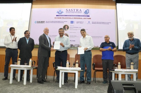
The report was formally launched in India at SASTRA University during the XX Nani Palkhiwala Memorial Lecture on April 4, marking a significant milestone in aligning industry, academia, and government stakeholders. The launch was led by Shri S. Krishnan, Secretary, Ministry of Electronics and Information Technology (MeitY), who highlighted the growing importance of semiconductors across AI, manufacturing, exports, and the upcoming ISM 2.0 framework.
The event also brought together key industry leaders, including Ranjan Bandyopadhyay, CHRO, Tata Electronics, and Suresh Babu, Managing Director, Caliber Interconnects, reinforcing the collaborative nature of the initiative.
A Clear Strategic Direction: “Shifting Left”
One of the central themes of the report is the concept of “shifting left”—a strategic move away from low-value assembly and testing toward advanced semiconductor packaging.
India currently operates from a near-zero base in semiconductor manufacturing, with much of the process expertise and supply chain located outside the country. The report argues that advanced packaging offers the most viable entry point to bridge this gap.
It further identifies advanced packaging as the next major inflection point in the global semiconductor industry, driven by system-level integration, heterogeneous architectures, and performance optimization .
Three Core Technology Domains
The report structures its roadmap around three critical domains:
Integrated Power Modules (IPM) for Power Electronics
Targeting applications such as electric vehicles and renewable energy, this domain aligns strongly with India’s domestic growth sectors.
Key findings include:
- System-level readiness at ~90%
- Packaging readiness at ~50%
- Fabrication readiness at ~40%
- Significant dependence on imported equipment
The report prioritizes EV applications, particularly two-wheelers and four-wheelers, with a focus on 400V systems suited to India’s cost-sensitive market .
Wafer-Level Packaging (WLP) for Displays
With India being a major consumer of display technologies, this domain focuses on packaging solutions for smartphones, TVs, automotive displays, and XR devices.
The report highlights:
- Reasonable capability in final assembly and testing
- Major gaps in display driver fabrication and module manufacturing
- Absence of a domestic glass substrate ecosystem
While recent industry partnerships indicate progress, the report stresses the need for sustained execution to avoid historical setbacks .
Glass and Organic Core Substrates
This is identified as one of the most critical and underdeveloped segments.
Key challenges include:
- Minimal domestic manufacturing capability
- Limited materials and equipment ecosystem
- Gaps in modelling, reliability, and large-scale production
At the same time, emerging technologies like glass core substrates offer India an opportunity to build capabilities in next-generation semiconductor platforms .
Manufacturing Readiness: A Data-Driven Baseline
The report uses the Manufacturing Readiness Level (MRL) framework to assess ecosystem maturity across multiple domains.
Strengths:
- Strong academic and research base
- Presence of global semiconductor players
- Growing demand across electronics and automotive sectors
Key gaps:
- Advanced packaging manufacturing infrastructure
- Local materials supply chain
- Equipment localization
- Pilot manufacturing lines
- Testing and reliability infrastructure
This structured assessment provides a clear baseline for tracking progress over the next decade.
Pre-Competitive Collaboration Model
A defining aspect of the INEMI initiative is its pre-competitive, consortium-driven approach.
This model enables:
- Collaboration without IP exchange
- Shared R&D and risk reduction
- Faster technology deployment
- Ecosystem-wide capability building
Participants include global semiconductor companies, Indian enterprises, equipment providers, materials suppliers, and leading academic institutions—creating a comprehensive value chain network.
From Roadmap to Execution
The report outlines a phased implementation plan:
- 2025: Ecosystem engagement and roadshows
- 2026: Working group formation and baseline assessment
- 2027: Launch of collaborative test vehicles
- 2028+: Pilot manufacturing and scale-up
The planned test vehicle programs in 2027 will play a critical role in validating manufacturing processes, testing new materials, and demonstrating packaging architectures across domains.
Cross-Domain Insights
Across all three domains, the report identifies common ecosystem characteristics:
- Strong design and research capabilities
- Weak manufacturing depth
- Heavy reliance on imports for materials and equipment
- Need for pilot lines and real-world validation
These insights reinforce the importance of a coordinated, long-term approach.
Conclusion
The INEMI 1Q26 Advanced Packaging Report stands out as a practical, execution-focused blueprint for India’s semiconductor ambitions. Its launch in India, backed by government leadership and industry participation, underscores the national importance of building a resilient semiconductor ecosystem.
By focusing on advanced packaging, adopting a collaborative model, and grounding its recommendations in manufacturing readiness metrics, the report provides a clear pathway for India to transition from design leadership to sustainable manufacturing capability.
As the ecosystem moves from roadmap to execution, the success of this initiative will depend on how effectively stakeholders translate this vision into action over the coming decade.