
Introduction
An astable multivibrator is a free-running oscillator that continuously alternates between two unstable states without the need for any external trigger. When power is applied, the transistors alternately switch from cut-off to saturation at a rate determined by the RC time constants of the coupling circuitry.
If the time constants are equal (R and C values are equal), a square wave is produced with a frequency of approximately 1 / (1.4RC). For this reason, an astable multivibrator is also known as a pulse generator or square wave generator.
The greater the value of the base load resistors (R2 and R3) compared to the collector load resistors (R1 and R4), the greater the current gain and the sharper the waveform edges. The astable multivibrator operates based on slight variations in the electrical characteristics of the transistors. When the supply is applied, one transistor turns ON slightly faster than the other, which initiates oscillations.
Construction of Astable Multivibrator
The circuit consists of two transistors, Q1 and Q2, connected in a feedback configuration. The capacitor C1 connects the collector of Q1 to the base of Q2, and capacitor C2 connects the collector of Q2 to the base of Q1.
The emitters of both transistors are connected to ground. The collector load resistors (R1 and R4) and the base biasing resistors (R2 and R3) have equal values. Similarly, the capacitors C1 and C2 also have equal values.
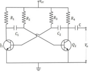
This symmetrical configuration ensures continuous oscillation between the two transistors.
Operation of Astable Multivibrator
Assume that when the power is first switched ON, transistor Q1 is conducting heavily and transistor Q2 is switched OFF. The collector of Q1 and the left plate of capacitor C1 are almost at 0 V. Since Q2 is OFF, its collector is at the supply voltage, and its base is also near 0 V because the capacitor is initially uncharged.
Now, capacitor C1 begins to charge through resistor R2. When the voltage on the base of Q2 reaches approximately +0.6 V, Q2 begins to conduct. As Q2 turns ON, its collector voltage drops, causing a sudden change in voltage across capacitor C2. This sudden change pulls down the base of Q1 to a negative voltage, turning Q1 OFF. As Q1 turns OFF, its collector voltage rises rapidly, which again causes a sudden change through capacitor C1, driving Q2 further ON.
This process continues as capacitor C2 now charges through R3. When the base voltage of Q1 again reaches approximately +0.6 V, Q1 turns ON and Q2 turns OFF. The cycle then repeats, producing continuous oscillations.
Frequency Calculation
The time taken for each capacitor to charge to the threshold voltage (around 0.6 – 0.7 V) is approximately:
t ≈ 0.7RC
Since two such changes occur in one complete cycle, the total time period (T) is:
T = 1.4RC
Therefore, the frequency of oscillation is:
f = 1 / 1.4RC
If C1 = C2 and R2 = R3, the mark-to-space ratio is 1:1 and a perfect square wave is generated.
Design Example
- Transistor used: BC107
- Collector current (IC(sat)) = 2 mA
- VCE = 2.7 V
- Collector resistors: RC1 = RC2
- Base current: IB(min) = IC / hFE
- Actual base current: IB = 5 × IB(min)
- Base-emitter voltage: VBE = 0.7 V
- R1 = R2 and C1 = C2
Waveforms
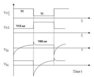
The output waveforms obtained at the collectors of Q1 and Q2 are square waves that are 180° out of phase with each other. These waveforms are used in clock generation and timing applications.
Advantages
- No external triggering is required
- Simple and easy circuit design
- Continuous operation
- Power efficient due to alternate switching
Disadvantages
- Energy absorption is more concentrated in the circuit
- Output signal has a relatively low energy level
- Duty cycle less than or equal to 50% is difficult to achieve
- Feedback does not provide full output to the input
Applications
- Amateur radio equipment and Morse code generators
- Timer circuits and analogue systems
- Television systems
- Pulse position modulation and frequency modulation
- Square wave and clock signal generation