• Home
  • About Us
  • Contact Us
Semiconductor for You
  • Home
  • Semiconductor News
  • Technology
    • Automotive
    • Consumer Electronics
    • IoT
    • Lighting
    • Power Management
    • Wireless
    • Personal Electronics
    • Hardware & Software
    • Research
    • Medical Electronics
    • Embedded Design
    • Aerospace & Defence
    • Artificial Intelligence
  • DIY Projects
  • Market
  • Industries
    • Renesas Electronics
  • Knowledge Base
  • Events
  • Tools
    • Resistor Color Code Calculator
No Result
View All Result
Semiconductor for You
No Result
View All Result
Home Articles

Construction of photodiode

Semiconductor For You by Semiconductor For You
July 2, 2021
in Articles
0
ADVERTISEMENT

The photodiode is a two terminal PN junction device which is operated in reverse bias. It has a small transparent window which allows light to strike the PN junction. The photodiode is a semiconductor device which is used to convert light which is fall on it to current. A photodiode is a semiconductor device with a PN junction and an intrinsic layer between p type and n layer.

It consists of built in lenses and optical filters with small or large surface areas.

The symbol of photodiode is shown in below.

photodiode
photodiode

Construction:

  • The basic construction of photodiode is shown in above fig.
  • The silicon photodiodes are constructed from single crystal silicon wafers.
  • A thin p layer is formed on the front surface of the device of thermal diffusion. N type silicon is a starting material.
  • The interface between the p layer and n layer is known as PN junction. To the front of the surface of the device small metal contacts are applied and the entire back is coated with a metal contact.
  • Anode is the front contact and the back contact is the cathode.
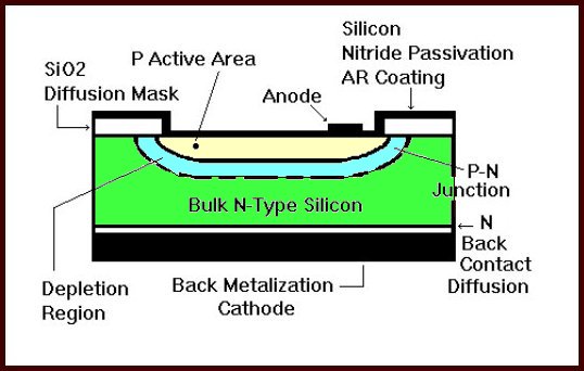
construction of photodiode
Content Protection by DMCA.com
Tags: photodiodeSemiconductors
Semiconductor For You

Semiconductor For You

Browse by Category

  • Aerospace and Defence
  • Articles
  • Automotive
  • Consumer-Electronics
  • Hardware & Software
  • Interview
  • IoT
  • Knowledge Base
  • Lighting
  • Market
  • personal-electronics
  • Power Management
  • Research
  • Semiconductor Events
  • Semiconductor News
  • Technology
  • Wireless
Semiconductor for You

Semiconductor For You is a resource hub for electronics engineers and industrialist. With its blend of
technology features, news and new product information, Semiconductor For You keeps designers and
managers up to date with the fastest moving industry in the world.

Follow Us

Browse by Category

  • Aerospace and Defence
  • Articles
  • Automotive
  • Consumer-Electronics
  • Hardware & Software
  • Interview
  • IoT
  • Knowledge Base
  • Lighting
  • Market
  • personal-electronics
  • Power Management
  • Research
  • Semiconductor Events
  • Semiconductor News
  • Technology
  • Wireless

Recent News

New SPI Absolute Encoder Supports 9 mm to 15.875 mm Motor Shafts

New SPI Absolute Encoder Supports 9 mm to 15.875 mm Motor Shafts

June 11, 2025
Infineon Secures the Future with 10 Billion Integrity Guard Chips Delivered

Infineon Secures the Future with 10 Billion Integrity Guard Chips Delivered

June 11, 2025
  • About
  • Advertise
  • Privacy & Policy
  • Contact

© 2022 Semiconductor For You

No Result
View All Result
  • Home
  • Semiconductor News
  • Technology
    • IoT
    • Wireless
    • Power Management
    • Automotive
    • Hardware & Software
  • Market
  • Knowledge Base
  • Tools
    • Resistor Color Code Calculator

© 2022 Semiconductor For You