• Home
  • About Us
  • Contact Us
Semiconductor for You
  • Home
  • Semiconductor News
  • Technology
    • Automotive
    • Consumer Electronics
    • IoT
    • Lighting
    • Power Management
    • Wireless
    • Personal Electronics
    • Hardware & Software
    • Research
    • Medical Electronics
    • Embedded Design
    • Aerospace & Defence
    • Artificial Intelligence
  • DIY Projects
  • Market
  • Industries
    • Renesas Electronics
  • Knowledge Base
  • Events
  • Tools
    • Resistor Color Code Calculator
No Result
View All Result
Semiconductor for You
No Result
View All Result
Home Articles

Depletion type N channel MOSFET

Semiconductor For You by Semiconductor For You
June 1, 2021
in Articles
0
ADVERTISEMENT

Depletion mode:

When the gate voltage is positive with respect to source, the depletion type MOSFET (metal oxide semiconductor field effect transistor) operates in depletion mode.

In the depletion type MOSFET, the device is normally ON at zero gate-source voltage. Such devices are used as load “resistors” in logic circuits. For the N type depletion load devices, the threshold voltage may be about –3 V. It could be turned off by pulling the gate 3 V negative.

Construction:
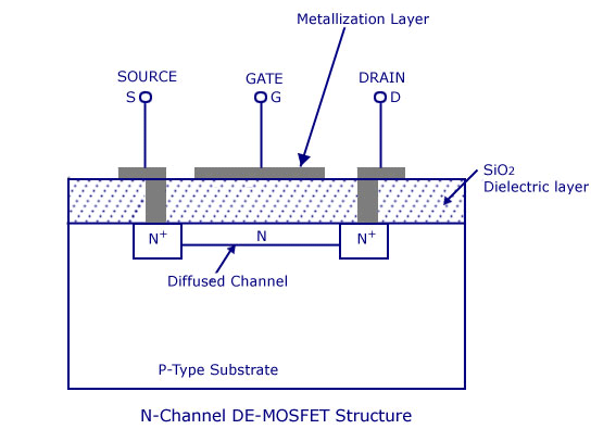
N-Channel DE-MOSFET Structure
  • The construction of depletion type N channel MOSFET (metal oxide semiconductor field effect transistor) is shown in above figure.
  • It consist conducting bar of N type silicon material with an insulated gate on the left and P region on the right.
  • The N channel is formed by distribution between the source and drain. The type of impurity for the channel is the same as for the source and the drain.
  • Here is a single P region which is called substrate or body. It physically reduces the conducting path to the narrow channel.
  • A thin layer of silicon dioxide is deposited on the left side of the N type channel. This layer insulates the gate from the channel. It has no PN junction.
Content Protection by DMCA.com
Tags: Semiconductors
Semiconductor For You

Semiconductor For You

Browse by Category

  • Aerospace and Defence
  • Articles
  • Automotive
  • Consumer-Electronics
  • Hardware & Software
  • Interview
  • IoT
  • Knowledge Base
  • Lighting
  • Market
  • personal-electronics
  • Power Management
  • Research
  • Semiconductor Events
  • Semiconductor News
  • Technology
  • Wireless
Semiconductor for You

Semiconductor For You is a resource hub for electronics engineers and industrialist. With its blend of
technology features, news and new product information, Semiconductor For You keeps designers and
managers up to date with the fastest moving industry in the world.

Follow Us

Browse by Category

  • Aerospace and Defence
  • Articles
  • Automotive
  • Consumer-Electronics
  • Hardware & Software
  • Interview
  • IoT
  • Knowledge Base
  • Lighting
  • Market
  • personal-electronics
  • Power Management
  • Research
  • Semiconductor Events
  • Semiconductor News
  • Technology
  • Wireless

Recent News

Inside the Future Home

Inside the Future Home

June 20, 2025
TDK acquires SoftEye

TDK acquires SoftEye

June 19, 2025
  • About
  • Advertise
  • Privacy & Policy
  • Contact

© 2022 Semiconductor For You

No Result
View All Result
  • Home
  • Semiconductor News
  • Technology
    • IoT
    • Wireless
    • Power Management
    • Automotive
    • Hardware & Software
  • Market
  • Knowledge Base
  • Tools
    • Resistor Color Code Calculator

© 2022 Semiconductor For You