• Home
  • About Us
  • Contact Us
Semiconductor for You
  • Home
  • Semiconductor News
  • Technology
    • Automotive
    • Consumer Electronics
    • IoT
    • Lighting
    • Power Management
    • Wireless
    • Personal Electronics
    • Hardware & Software
    • Research
    • Medical Electronics
    • Embedded Design
    • Aerospace & Defence
    • Artificial Intelligence
  • DIY Projects
  • Market
  • Industries
    • Renesas Electronics
  • Knowledge Base
  • Events
  • Tools
    • Resistor Color Code Calculator
No Result
View All Result
Semiconductor for You
No Result
View All Result
Home Knowledge Base

Fabrication of p-n Junctions -Thermal oxidation

Semiconductor For You by Semiconductor For You
May 13, 2019
in Knowledge Base
0
ADVERTISEMENT

Although we know that how devices work rather than how they are made, it is instructive to have an overview of the fabrication process in order to appreciate device physics. We also know that  how single-crystal substrates and epitaxial layers needed for high quality devices are grown, and how the doping can be varied as a function of depth.

Fabrication of p-n Junctions: Thermal oxidation:

  • However, we have not discussed how doping can be varied laterally across the surface, which is key to making integrated circuits on a wafer.
  • Hence, it is necessary to be able to form patterned masks on the wafer corresponding to the circuitry, and introduce the dopants selectively through windows in the mask.
  • We will first briefly describe the major process steps that form the underpinnings of modern integrated circuit manufacturing.
  • Relatively few unit process steps can be used in different permutations and combinations to make everything from simple diodes to the most complex microprocessors.


Thermal Oxidation:

  • Many fabrication steps involve heating up the wafer in order to enhance a chemical process. An important example of this is thermal oxidation of Si to form Si02.
  • This involves placing a batch of wafers in a clean silica (quartz) tube which can be heated to very high temperatures (~800-1000°C) using heating coils in a furnace with ceramic brick insulating liners.
  • An oxygen containing gas such as dry o2 or H2O is flowed into the tube at atmospheric pressure, and flowed out at the other end.
  • Traditionally, horizontal furnaces were used. More recently, it has become common to employ vertical furnaces.
  • A batch of Si wafers is placed in the silica wafer holders, each facing down to minimize particulate contamination.
  • The wafers are then moved into the furnace.
  • The gases flow in from the top and flow out at the bottom, providing more uniform flow than in conventional horizontal furnaces.

The overall reactions that occur during oxidation are:


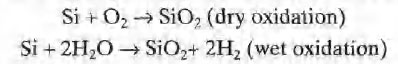
  • In both cases. Si is consumed from the surface of the substrate.
  • For every micron of Si02 grown, 0.44 μm of Si is consumed, leading to a 2.2 X volume expansion of the consumed layer upon oxidation.
  • The oxidation proceeds by having the oxidant (02 or H2o) molecules diffuse through the already grown oxide to the Si-Si02interface, where the above reactions take place.
  • One of the very important reasons why Si integrated circuits exist (and by extension why modern computers exist) is that a stable thermal oxide can be grown on Si with excellent interface electrical properties.
  • Other semiconductor materials do not have such a useful native oxide.
  • We can argue that modern electronics and computer technology owe their existence to this simple oxidation process.
Content Protection by DMCA.com
Semiconductor For You

Semiconductor For You

Browse by Category

  • Aerospace and Defence
  • Articles
  • Automotive
  • Consumer-Electronics
  • Hardware & Software
  • Interview
  • IoT
  • Knowledge Base
  • Lighting
  • Market
  • personal-electronics
  • Power Management
  • Research
  • Semiconductor Events
  • Semiconductor News
  • Technology
  • Wireless
Semiconductor for You

Semiconductor For You is a resource hub for electronics engineers and industrialist. With its blend of
technology features, news and new product information, Semiconductor For You keeps designers and
managers up to date with the fastest moving industry in the world.

Follow Us

Browse by Category

  • Aerospace and Defence
  • Articles
  • Automotive
  • Consumer-Electronics
  • Hardware & Software
  • Interview
  • IoT
  • Knowledge Base
  • Lighting
  • Market
  • personal-electronics
  • Power Management
  • Research
  • Semiconductor Events
  • Semiconductor News
  • Technology
  • Wireless

Recent News

New SPI Absolute Encoder Supports 9 mm to 15.875 mm Motor Shafts

New SPI Absolute Encoder Supports 9 mm to 15.875 mm Motor Shafts

June 11, 2025
Infineon Secures the Future with 10 Billion Integrity Guard Chips Delivered

Infineon Secures the Future with 10 Billion Integrity Guard Chips Delivered

June 11, 2025
  • About
  • Advertise
  • Privacy & Policy
  • Contact

© 2022 Semiconductor For You

No Result
View All Result
  • Home
  • Semiconductor News
  • Technology
    • IoT
    • Wireless
    • Power Management
    • Automotive
    • Hardware & Software
  • Market
  • Knowledge Base
  • Tools
    • Resistor Color Code Calculator

© 2022 Semiconductor For You