


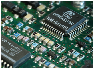
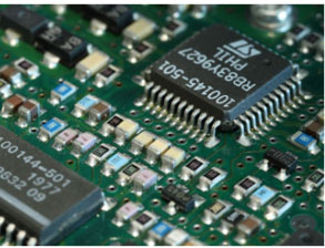

PCB is a printed circuit board. As mention in its name, PCB is a board on which the circuit is printed. In other words, PCB mechanically supports and electrically connects electronic components using conductive traces, pads, and other features etched from copper sheets laminated onto a non-conductive substrate.
Printed Circuited board is the most common name which is also called “printed wiring board” or “printed wiring cards”. If we say in an easier way that is when we open any electronic item or equipment like TV, remote, laptops, etc. There is a green-colored board where the number of electronic components mounted. It’s called PCB.

Before the invention of PCB, Electronic components are connected with an electric wire that is point-to-point wiring/construction was used. That’s why circuitry in electronic equipment was very complex. All the components are connected with wires only because this circuit looks like a big tangled mess. And if is there is any problem arise, it becomes very difficult to identify the cause and to resolve or change any components or wire. It was a difficult process and takes a long duration of time to do. This point-to-point wiring makes the circuit large, heavy and fragile. That’s why old TVs or computers were thick and bulky. But now the problem is solved. Over the years, numerous adjustments and changes were made to improve the concepts. The number of components is fixed small area in PCB. PCBs have gotten smaller in size and more powerful. The works of electrical wire are now done by copper traces. Copper traces connect the electrical components between them. These copper traces can easily be seen through the naked eye. In PCB’s, two types of materials are used. The first one is conductive material another one is dielectric materials. In conductive material, copper is used and dielectric material fiberglass is used. The layer of these materials is stacked one above the other. These PCB’s are widely used as the basis for electronic circuits.