
- The MC34063A Series is a monolithic control circuit that contains all of the primary functions needed for Dc to DC converters. An internal temperature compensated reference, comparator, controlled duty cycle oscillator with an active current limit circuit, driver, and high current output switch are all part of these devices.
- This series was created specifically to be used in step-down, step-up, and voltage inverting applications with a minimal number of external components.
The MC34063 includes the following components
- Temperature-compensated reference voltage.
- Oscillator.
- Active peak-current limit.
- Output switch.
- Output voltage-sense comparator.
Block Diagram of the MC34063 DC to DC Converter
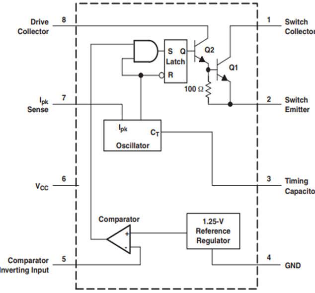
- The oscillator is made up of a current source and sink that charge and discharge the external timing capacitor (CT) between two preset thresholds. Charge and discharge currents are typically 35 mA and 200 mA, respectively, yielding a 6:1 ratio. As a result, the ramp-up period is six times longer than the ramp-down period. The upper threshold is approximately equal to 1.25 V, and the lower threshold is approximately equal to 0.75 V. The oscillator runs continuously at a rate determined by CT.
- A logic 1 is present at the AND gate’s A input during the ramp-up portion of the cycle. If the switching regulator’s output voltage is less than nominal, logic 1 is also present at the B input. This condition enables the driver and output switch to conduct by setting the latch and causing the Q output to be a logic 1. When the oscillator reaches its upper threshold, CT begins to discharge, and a logic 0 appears at the AND gate’s A input. This logic level is also linked to an inverter, the output of which sends a logic 1 to the latch’s reset input. This condition causes Q to go low, effectively turning off the driver and output switch.
- The comparator output can only set the latch during CT ramp up and can initiate a partial or full-on cycle of output switch conduction. The comparator cannot reset the latch once it has set it. The latch remains in place until CT begins to ramp down. As a result, the comparator can initiate but not terminate output switch conduction, and the latch is always reset when CT begins ramping down. When the switching regulator’s output voltage exceeds the nominal, the comparator’s output is logic 0.
- The comparator’s output can inhibit a portion of the output switch on cycle, a complete cycle, a complete cycle plus a portion of one cycle, or multiple cycles under these conditions, a complete cycle plus a portion of one cycle, multiple cycles, or multiple cycles plus a portion of one cycle.
Pin configurations
The pin diagram of MC34063 DC to DC converter is shown below.
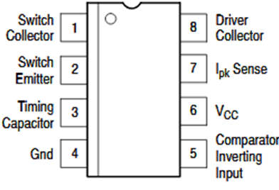
- Switch Collector – Internal transistor collector pin (Output Voltage pin).
- Switch Emitter – Internal Transistors’ Emitter Pin.
- Timing Capacitor – Connect to the capacitor that determines the switching frequency.
- Ground – Connected to ground.
- Comparator Inverting Input – Used to set the output voltage.
- Vcc – Input voltage is fed to this pin.
- Speak Sense – Used to set the output current.
- Driver Collector – Collector pin of switching transistor.
Features and Specifications
- Input voltage range: 3.0 V to 40 V.
- Standby current is low.
- Current is limited.
- Switch current up to 1.5 A.
- Adjustable output voltage.
- Frequency operation is limited to 100 kHz.
- 2 percent precision Reference.
- NCV is an AECQ100 qualified and PPAP capable prefix for automotive and other applications requiring unique site and control change requirements.
- These products are PbFree, HalogenFree/BFRFree, and RoHS Compliant.
Applications of MC34063 DC to DC Converter
- The MC34063A is a DC-DC converter integrated circuit that is commonly used in the design of Buck (step-down), Boost (Step-UP), or Inverter (DC to AC) circuits.
- It is an industrial standard IC that is used to regulate 5V for mobile phones in automobile phone chargers.
- The IC’s input voltage ranges from 3V to 40V, and its output voltage ranges from 1.25V to 40V with a maximum output current of 1.5A. If you are looking to design a DC-DC converter with the above specifications, the MC34063A may come in handy.