• Home
  • About Us
  • Contact Us
Semiconductor for You
  • Home
  • Semiconductor News
  • Technology
    • Automotive
    • Consumer Electronics
    • IoT
    • Lighting
    • Power Management
    • Wireless
    • Personal Electronics
    • Hardware & Software
    • Research
    • Medical Electronics
    • Embedded Design
    • Aerospace & Defence
    • Artificial Intelligence
  • DIY Projects
  • Market
  • Industries
    • Renesas Electronics
  • Knowledge Base
  • Events
  • Tools
    • Resistor Color Code Calculator
No Result
View All Result
Semiconductor for You
No Result
View All Result
Home Knowledge Base

Power MOSFETs

Semiconductor For You by Semiconductor For You
May 25, 2021
in Knowledge Base
0
ADVERTISEMENT

In general, power MOSFETs employ thicker oxides, deeper junctions and have longer channel lengths. These generally post a penalty on device performance such as transconductance (gm) and speed (fT). Nevertheless, power applications from MOSFETs have been on the rise, for example, due to the increasing demand of cellular phones and cellular base stations which require extra high voltage.

Power MOSFETs (Metal-Oxide Semiconductor Field Effect Transistors) are three terminal silicon devices that function by applying signal to the gate that controls current conduction between source and drain. Their current conduction capabilities are up to several tens of amperes with breakdown voltage rating of 10V to 1000V.

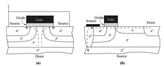
DMOS (Double-Diffused MOS)

As the name implies, in the DMOS transistor the channel length is determined by the higher diffusion rate of the P-doping compared to the N-doping of the source. The p-diffusion serves as channel doping and has good punch through control. The channel is followed by a lightly doped n- – drift region.

This drift region is long compared to the channel, and it minimizes the peak electric field in this region by maintaining a uniform field. Usually the drain is located at the substrate contact. The field near the drain is the same as in the drift region , so multiplication, avalanche breakdown and oxide charging are less compared to conventional MOSFETs.

LDMOS (Laterally Diffused MOS)

The LDMOS has a lateral current flow pattern which is major difference from DMOS. The drift region here is an implanted horizontal region. Such a horizontal arrangement enables thin- substrate to deplete this drift region at high drain bias. In low drain bias its higher doping gives lower series resistance.

Drift region behaves like nonlinear resistor. Its resistance determined by 1/nqµ at low drain bias. At high drain bias, the region is fdly depleted so a large voltage drop can be supported this concept called Reduce Surface Field (RESURF) technology.

Content Protection by DMCA.com
Tags: Powervoltage
Semiconductor For You

Semiconductor For You

Browse by Category

  • Aerospace and Defence
  • Articles
  • Automotive
  • Consumer-Electronics
  • Hardware & Software
  • Interview
  • IoT
  • Knowledge Base
  • Lighting
  • Market
  • personal-electronics
  • Power Management
  • Research
  • Semiconductor Events
  • Semiconductor News
  • Technology
  • Wireless
Semiconductor for You

Semiconductor For You is a resource hub for electronics engineers and industrialist. With its blend of
technology features, news and new product information, Semiconductor For You keeps designers and
managers up to date with the fastest moving industry in the world.

Follow Us

Browse by Category

  • Aerospace and Defence
  • Articles
  • Automotive
  • Consumer-Electronics
  • Hardware & Software
  • Interview
  • IoT
  • Knowledge Base
  • Lighting
  • Market
  • personal-electronics
  • Power Management
  • Research
  • Semiconductor Events
  • Semiconductor News
  • Technology
  • Wireless

Recent News

New SPI Absolute Encoder Supports 9 mm to 15.875 mm Motor Shafts

New SPI Absolute Encoder Supports 9 mm to 15.875 mm Motor Shafts

June 11, 2025
Infineon Secures the Future with 10 Billion Integrity Guard Chips Delivered

Infineon Secures the Future with 10 Billion Integrity Guard Chips Delivered

June 11, 2025
  • About
  • Advertise
  • Privacy & Policy
  • Contact

© 2022 Semiconductor For You

No Result
View All Result
  • Home
  • Semiconductor News
  • Technology
    • IoT
    • Wireless
    • Power Management
    • Automotive
    • Hardware & Software
  • Market
  • Knowledge Base
  • Tools
    • Resistor Color Code Calculator

© 2022 Semiconductor For You