• Home
  • About Us
  • Contact Us
Semiconductor for You
  • Home
  • Semiconductor News
  • Technology
    • Automotive
    • Consumer Electronics
    • IoT
    • Lighting
    • Power Management
    • Wireless
    • Personal Electronics
    • Hardware & Software
    • Research
    • Medical Electronics
    • Embedded Design
    • Aerospace & Defence
    • Artificial Intelligence
  • DIY Projects
  • Market
  • Industries
    • Renesas Electronics
  • Knowledge Base
  • Events
  • Tools
    • Resistor Color Code Calculator
No Result
View All Result
Semiconductor for You
No Result
View All Result
Home Articles

V I Characteristics of UJT

Semiconductor For You by Semiconductor For You
May 27, 2021
in Articles
0
ADVERTISEMENT
  • The V I Characteristics of UJT (unijunction transistor) is show in above fig.
  • The emitter voltageVE is applied between emitter E and base B1. VE is positive with respect B1. Let increasing this voltage from zero.
  • The PN junction is reverse biased and emitter current IE is negative as long as the emitter voltage VE< η VBB as shown by the curve PS.
  • The current flowing are very close to the reverse leakage current of PN junction reverse biased.
  • At point B, the emitter voltage VEis equal to ηVBB +VD the PN junction is forward biased and UJT starts conducting.
  • The point B is known as the peak pointand the voltage and current across its known as peak point voltage (VP) and peak point current (IP) respectively.
  • The emitter voltage VE decreases with increase in emitter current IE. Due to drop in resistance rb1 with increase in the value of IE reduction in voltage across UJT.
  • Thus the device exhibits a negative resistance region as shown by the curve BC.
  • The entire base region is saturated at point C and rb1 does not decrease any more. As shown in curve CQ, the rise in voltage VEso further increase in IE.
  • The point C is known as valley voltageand the voltage and current across is known as valley voltage (VV) and valley current (IV).
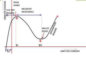
V I Characteristics of UJT
Content Protection by DMCA.com
Semiconductor For You

Semiconductor For You

Browse by Category

  • Aerospace and Defence
  • Articles
  • Automotive
  • Consumer-Electronics
  • Hardware & Software
  • Interview
  • IoT
  • Knowledge Base
  • Lighting
  • Market
  • personal-electronics
  • Power Management
  • Research
  • Semiconductor Events
  • Semiconductor News
  • Technology
  • Wireless
Semiconductor for You

Semiconductor For You is a resource hub for electronics engineers and industrialist. With its blend of
technology features, news and new product information, Semiconductor For You keeps designers and
managers up to date with the fastest moving industry in the world.

Follow Us

Browse by Category

  • Aerospace and Defence
  • Articles
  • Automotive
  • Consumer-Electronics
  • Hardware & Software
  • Interview
  • IoT
  • Knowledge Base
  • Lighting
  • Market
  • personal-electronics
  • Power Management
  • Research
  • Semiconductor Events
  • Semiconductor News
  • Technology
  • Wireless

Recent News

Inside the Future Home

Inside the Future Home

June 20, 2025
TDK acquires SoftEye

TDK acquires SoftEye

June 19, 2025
  • About
  • Advertise
  • Privacy & Policy
  • Contact

© 2022 Semiconductor For You

No Result
View All Result
  • Home
  • Semiconductor News
  • Technology
    • IoT
    • Wireless
    • Power Management
    • Automotive
    • Hardware & Software
  • Market
  • Knowledge Base
  • Tools
    • Resistor Color Code Calculator

© 2022 Semiconductor For You