• Home
  • About Us
  • Contact Us
Semiconductor for You
  • Home
  • Semiconductor News
  • Technology
    • Automotive
    • Consumer Electronics
    • IoT
    • Lighting
    • Power Management
    • Wireless
    • Personal Electronics
    • Hardware & Software
    • Research
    • Medical Electronics
    • Embedded Design
    • Aerospace & Defence
    • Artificial Intelligence
  • DIY Projects
  • Market
  • Industries
    • Renesas Electronics
  • Knowledge Base
  • Events
  • Tools
    • Resistor Color Code Calculator
No Result
View All Result
Semiconductor for You
No Result
View All Result
Home Knowledge Base

What is a 74HC595 Shift Register & Its Working

Mrinali Sharma by Mrinali Sharma
August 25, 2022
in Knowledge Base
0
ADVERTISEMENT
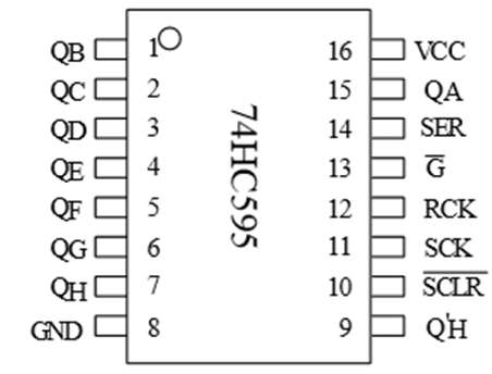
  • 74HC595 IC is a 16-pin shift register IC consisting of a D-type latch along with a shift register inside the chip.
  • It receives serial input data and then sends out this data through parallel pins.
  • In addition to parallel outputs, it also provides a serial output. It has independent clock inputs for the shift register and D latch.

Features

  • It is a shift register with 8-bit serial input and 8-bit serial or 3-state parallel outputs.
  • The operating voltage of this IC is from 2V to 6V.
  • The output voltage is equal to the operating voltage of this IC.

Working


  • 74HC595 Shift Register
  • 74HC595 shift register consists of two registers a shift register and a storage register. Both are 8-bit wide.
  • The first one is responsible to accept data input on every positive edge of the clock and it keeps receiving data.
  • But data from the shift register transfer to the storage register only when we apply an active high signal to the latch input pin.
  • It has 8outputs and 3input pins which include a data pin, storage resistor clock pin, and shift register clock pin.
  • Connect pin8 to ground and pin16 to +5V voltage supply.
  • The output enable pin (~OE) should be grounded to enable the output pins of the shift register.
  • The master reset pin will clear the memory of a shift register if it is applied with a low signal.
  • That’s why it should be kept high.
  • When the positive edge transition occurs on pin 11, the shift register will accept the inputs applied on the data line.
  • The outputs of the storage register are connected to the input pins of the D-latch/storage resistor.
  • These inputs are updated on the latch output when a positive edge transition occurs at pin 12.
Content Protection by DMCA.com
Mrinali Sharma

Mrinali Sharma

Browse by Category

  • Aerospace and Defence
  • Articles
  • Automotive
  • Consumer-Electronics
  • Hardware & Software
  • Interview
  • IoT
  • Knowledge Base
  • Lighting
  • Market
  • personal-electronics
  • Power Management
  • Research
  • Semiconductor Events
  • Semiconductor News
  • Technology
  • Wireless
Semiconductor for You

Semiconductor For You is a resource hub for electronics engineers and industrialist. With its blend of
technology features, news and new product information, Semiconductor For You keeps designers and
managers up to date with the fastest moving industry in the world.

Follow Us

Browse by Category

  • Aerospace and Defence
  • Articles
  • Automotive
  • Consumer-Electronics
  • Hardware & Software
  • Interview
  • IoT
  • Knowledge Base
  • Lighting
  • Market
  • personal-electronics
  • Power Management
  • Research
  • Semiconductor Events
  • Semiconductor News
  • Technology
  • Wireless

Recent News

New SPI Absolute Encoder Supports 9 mm to 15.875 mm Motor Shafts

New SPI Absolute Encoder Supports 9 mm to 15.875 mm Motor Shafts

June 11, 2025
Infineon Secures the Future with 10 Billion Integrity Guard Chips Delivered

Infineon Secures the Future with 10 Billion Integrity Guard Chips Delivered

June 11, 2025
  • About
  • Advertise
  • Privacy & Policy
  • Contact

© 2022 Semiconductor For You

No Result
View All Result
  • Home
  • Semiconductor News
  • Technology
    • IoT
    • Wireless
    • Power Management
    • Automotive
    • Hardware & Software
  • Market
  • Knowledge Base
  • Tools
    • Resistor Color Code Calculator

© 2022 Semiconductor For You