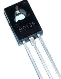
- The BD136 is another PNP and NPN transistor in the BD13x series. This transistor is housed in a TO-126 package. It can handle or drive a maximum collector current of -1.5A and a maximum pulse current of 2A, but it requires a suitable heatsink to function properly.
- Because the BD136 is a PNP transistor, the collector and emitter are closed (forward-biased) when the base pin is held at the ground and open (reverse biased) when a signal is applied to the base pin. A PNP transistor differs from an NPN transistor in this regard.
- The base pin’s small input current is used to generate a large output current at the other two terminals. This procedure is used for amplification.
- BD136 is made up of three layers, one of which is n-doped and the other two of which are p-doped. Between the two p-doped layers is an n-doped layer.
- The base pin is represented by the n-layer, while the emitter and collector are represented by the other two layers.
- Though both electrons and holes are important in conductivity because this is a PNP transistor, the majority of carriers are holes, as opposed to an NPN transistor, where the majority of carriers are electrons.
- The base pin is the main terminal responsible for the entire transistor action in both cases. The base pin functions as a valve, regulating the number of holes in PNP transistors and electrons in NPN transistors.
- It is important to note that NPN transistors are preferred over PNP transistors for amplification purposes because electron mobility in NPN transistors is better and faster than hole mobility in PNP transistors.
Pin Configuration
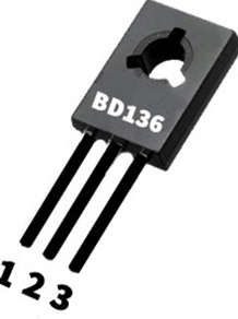
- The pin diagram of the BD136 medium power PNP transistor is shown below.
| Pin No. | Pin Name | Description |
|---|---|---|
| 1 | Emitter | Current Drains out through emitter, normally connected to ground. |
| 2 | Collector | Current flows in through collector, normally connected to load. |
| 3 | Base | Controls the biasing of the transistor; used to turn the transistor ON or OFF. |
Working
- The working principle of this PNP transistor is straightforward and similar to that of an NPN transistor. In addition, in an NPN transistor, the base pin is positive, whereas, in a PNP transistor, it is negative.
- When there is no current at the base side, the transistor is turned on and both the emitter and collector terminals are forward biased.
- When there is current at the base terminal, the transistor is turned off, resulting in reverse bias on both the collector and emitter sides.
- Remember that NPN transistors are preferred over PNP transistors for amplification because electron mobility is better and faster than hole mobility in the PNP transistor.
Applications of BD136 Transistor
- Collector Current (IC) Maximum: -5A.
- Collector-Emitter Voltage (VCE) Maximum: -45V.
- -45V is the maximum collector-base voltage (VCB).
- -5V is the maximum emitter-base voltage (VEBO).
- 5 Watt is the maximum collector dissipation (Pc).
- 190 MHz is the maximum transition frequency (fT).
- DC Current Gain (hFE) Minimum & Maximum: 25 – 250.
- Max Temperatures for storage and operation should range from -55 to +150 degrees Celsius.
- TO-126 is the package type.
- PNP is the transistor type.